
Vespel® Dual Gas Components for Semiconductor Plasma Equipment: Material Selection, Precision Machining, and Application Case Study
In semiconductor plasma etching, thin-film deposition, and other vacuum-based processes, process gases must be delivered accurately and consistently to specific areas inside the equipment. In addition to the main gas delivery system, many semiconductor tools rely on small but critical gas-guiding and gas-distribution components.
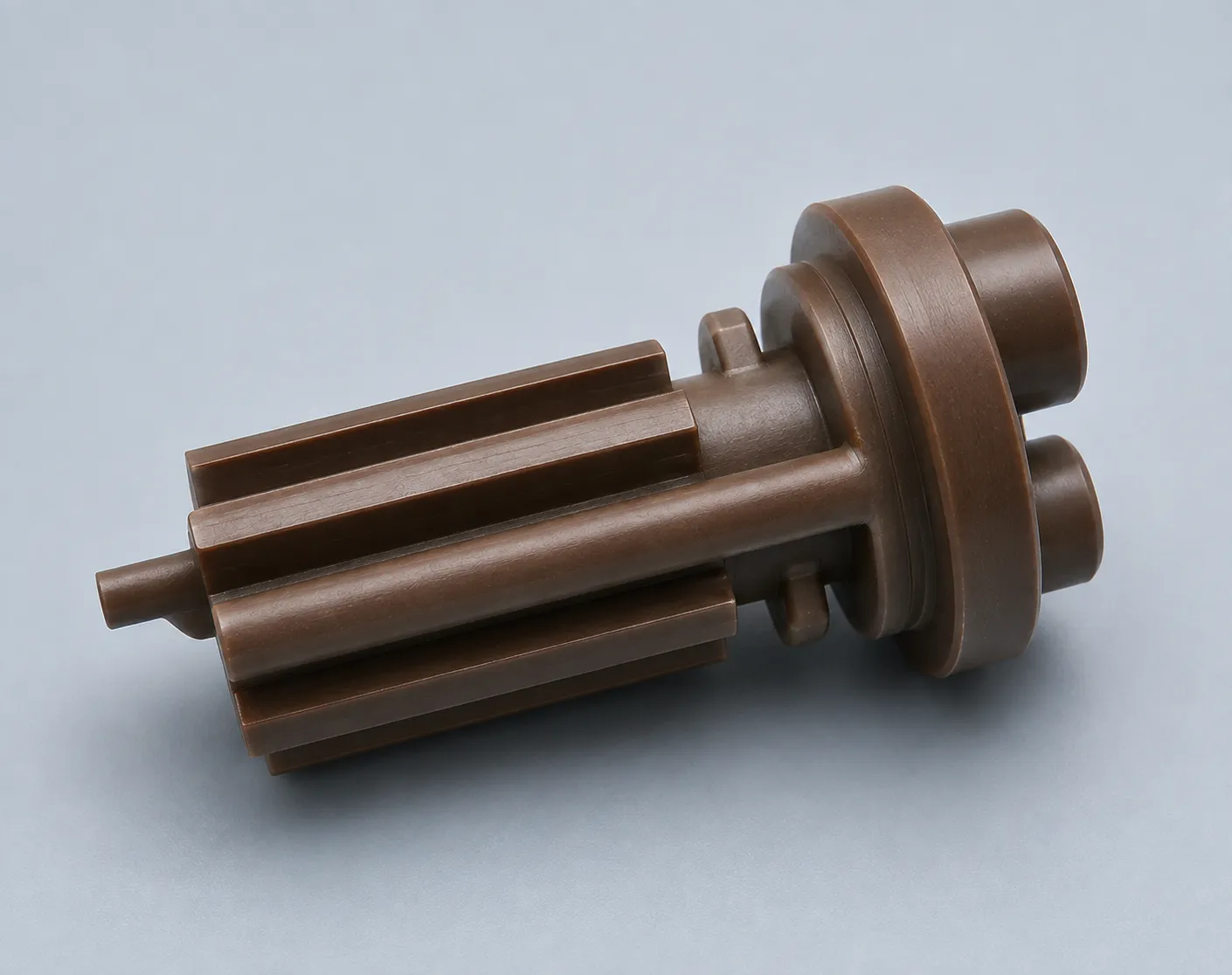
A Dual Gas component is one example of this type of precision part. These components may feature stepped diameters, longitudinal slots, thin supporting ribs, and internal gas passages. In addition to dimensional accuracy, the material must also withstand demanding conditions such as elevated temperatures, vacuum environments, electrical insulation requirements, and strict cleanliness expectations.
For certain semiconductor plasma applications, DuPont™ Vespel® polyimide is selected because of its excellent thermal stability, dimensional stability, electrical insulation properties, and suitability for vacuum environments.
What Is a Dual Gas Component?
Dual Gas components are commonly used for gas guidance, distribution, separation, positioning, or structural support within semiconductor plasma processing equipment.
Depending on the equipment design, the component may contain axial holes, radial holes, internal passages, or multiple gas channels. These internal features work together with external slots and openings to direct process gases toward designated areas.
For this reason, manufacturing a Dual Gas component involves more than simply machining the external geometry.
Dimensions such as outer diameter, length, slot width, positioning surfaces, and concentricity must be carefully controlled. At the same time, the diameter, position, cleanliness, and completeness of internal gas passages can directly affect gas flow behavior.
Although these components are often relatively small, they combine material requirements, precision machining challenges, and functional gas-flow considerations within a single part.
Application Case Study: Small Dual Gas Component for LAM Plasma Processing Environments
One representative example is a small gas-guiding component used in a LAM plasma processing environment.
This type of Dual Gas component can be used for process gas guidance, positioning, and support within plasma equipment. Depending on the actual operating conditions, materials such as Vespel®, PEEK, or other high-performance engineering polymers may be considered.
The component may appear simple due to its small overall size, but its geometry can be relatively complex.
Typical features include multiple stepped diameters, annular sections, and several narrow longitudinal slots extending along the body. After these slots are machined, thin and elongated supporting ribs remain between them.
As machining progresses and more material is removed, the local stiffness of the component gradually decreases. This means that cutting forces, machining sequence, tool sharpness, and workholding conditions must be carefully managed to minimize rib deformation and dimensional variation.
The internal gas passage is another critical feature.
If the design contains micro-holes, deep holes, radial holes, or intersecting gas channels, the machining process must control not only the hole diameter but also the position and relationship between each passage.
The real manufacturing challenge is therefore not simply machining Vespel® into the correct external shape. It is maintaining several critical characteristics at the same time:
- Dimensional accuracy and concentricity
- Consistency of longitudinal slots and thin ribs
- Correct location and integrity of gas passages
- Burr control around micro-holes and internal channels
- Cleanliness suitable for semiconductor equipment
- Stable performance after installation
These factors are essential for components used in semiconductor plasma environments.
Why Is Vespel® Selected?
Vespel® is a family of high-performance polyimide materials developed by DuPont.
Common engineering plastics such as POM, nylon, and other standard polymers provide good machinability and cost advantages. However, when a component must simultaneously operate under elevated temperatures, vacuum conditions, dimensional constraints, and electrical insulation requirements, these conventional materials may become less suitable.
Vespel® is designed for more demanding environments and is widely used in semiconductor, vacuum, aerospace, and high-temperature mechanical applications.
Vespel® SP-1 is one of the most commonly recognized grades. It is an unfilled polyimide with excellent mechanical, thermal, and electrical insulation properties.
Unlike conventional thermoplastics, Vespel® SP-1 does not exhibit a typical melting behavior during service. It can maintain useful mechanical and dimensional performance at temperatures significantly higher than many common engineering plastics.
Key Advantages of Vespel® in Semiconductor Equipment
- Excellent High-Temperature Performance
Certain areas inside plasma processing equipment can be exposed to elevated temperatures.
For components installed near heat sources or plasma processing zones, it is important that the material maintains its mechanical properties and dimensional stability as temperatures increase.
Vespel® offers excellent thermal performance compared with many conventional engineering plastics, making it suitable for demanding semiconductor applications.
- Good Dimensional Stability
Dual Gas components may include multiple stepped diameters, positioning surfaces, narrow slots, thin ribs, and precision mating features.
If the material experiences excessive dimensional change under temperature or long-term mechanical loading, alignment and gas delivery performance may be affected.
The low creep and good dimensional stability of Vespel® make it suitable for precision equipment components that require reliable long-term performance.
- Excellent Electrical Insulation
Unfilled Vespel® SP-1 provides excellent electrical insulation properties.
This can be particularly valuable in plasma systems, vacuum chambers, and other semiconductor equipment where electrical isolation between metallic components is required.
- Suitable for Vacuum Environments
Vespel® is well known for its low-outgassing characteristics and has a long history of use in vacuum applications.
In semiconductor processing equipment, excessive outgassing from polymer components may introduce unwanted contaminants into the process environment. Material selection is therefore particularly important for parts installed inside or near vacuum chambers.
- Suitable for Precision CNC Machining
Compared with engineering ceramics such as alumina or zirconia, Vespel® can be machined using conventional CNC turning, milling, drilling, and precision finishing processes.
This allows designers to create complex geometries including stepped diameters, slots, micro-holes, and internal passages while maintaining relatively high design flexibility.
CNC Machining Challenges of Dual Gas Components
Vespel® itself is not considered extremely difficult to machine.
The main manufacturing challenges typically come from the geometry of the component, particularly when the design combines small dimensions, thin structures, and internal gas passages.
Longitudinal Slots and Thin Rib Machining
Dual Gas components may feature multiple long slots extending along the body.
As each slot is machined, the remaining material forms long and relatively thin ribs. The rigidity of these ribs decreases as more surrounding material is removed.
If cutting forces, tool paths, or clamping methods are not properly controlled, the ribs may deflect slightly during machining, causing dimensional inconsistency or poor surface quality.
A carefully planned sequence of rough machining and finishing is therefore important for maintaining stability.
Micro-Holes and Gas Passages
The internal gas passages are among the most functionally important features of Dual Gas components.
If the design includes small-diameter holes, high aspect-ratio holes, radial holes, or intersecting channels, the machining process must control both geometry and cleanliness.
Even a small burr or machining chip remaining inside a gas passage may affect local gas flow or partially obstruct the channel.
For this reason, internal deburring, cleaning, and inspection are important steps after machining.
Concentricity and Positioning Accuracy
Many Dual Gas components contain several cylindrical diameters and stepped features that mate with other parts inside the equipment.
Maintaining a consistent machining datum helps minimize errors caused by repeated setups and ensures that the cylindrical sections, gas features, and positioning surfaces remain correctly aligned.
Burr and Particle Control
A small amount of residual burr may be acceptable in some general industrial plastic parts.
Semiconductor equipment is different.
Loose burrs around slots, ribs, or gas holes can become particle sources during operation. Precision deburring, cleaning, and final inspection are therefore important parts of the manufacturing process.
Vespel® SP-1 vs. PEEK for Dual Gas Components
Not every Dual Gas component must be manufactured from Vespel®.
The material should be selected according to operating temperature, vacuum conditions, chemical exposure, dimensional stability requirements, and cost.
| Property | Vespel® SP-1 | PEEK |
| Material family | Polyimide | Polyether Ether Ketone |
| High-temperature performance | Excellent | Very good |
| High-temperature dimensional stability | Excellent | Good |
| Electrical insulation | Excellent | Excellent |
| Vacuum suitability | Excellent | Good |
| CNC machinability | Good | Good |
| Material cost | Higher | Relatively lower |
| Typical selection criteria | High temperature, vacuum, dimensional stability | General semiconductor equipment, chemical resistance, cost efficiency |
When the operating temperature is relatively moderate and PEEK already satisfies the functional requirements, PEEK can provide a practical balance between performance, availability, and cost.
However, when the component operates in a more demanding plasma or vacuum environment and requires improved thermal performance, dimensional stability, low outgassing, and long-term reliability, Vespel® may be a more suitable choice.
It is also important to understand that Vespel® includes multiple grades.
Vespel® SP-1 is an unfilled polyimide that is commonly selected for thermal and electrical insulation applications, while grades such as SP-21 and SP-22 incorporate fillers to modify wear, friction, or dimensional characteristics.
Therefore, if a drawing specifies Vespel® SP-1, it should not automatically be replaced by another Vespel® grade or a generic polyimide material without confirming the actual application requirements.
Semiconductor Vespel® Parts Require More Than Standard Plastic Machining
From a machining perspective, Vespel® is a relatively machinable high-performance polymer.
However, semiconductor applications introduce additional requirements beyond basic dimensional tolerances.
For Dual Gas components, gas distributors, wafer guides, insulators, spacers, and other plasma equipment parts, the manufacturing process may also need to consider:
- Thin-wall and thin-rib deformation
- Micro-hole quality
- Internal gas passage integrity
- Concentricity and positional accuracy
- Burr control
- Particle control
- Material traceability
- Cleaning requirements
A successful manufacturing process therefore requires consideration of material characteristics, workholding, cutting tools, machining sequence, inspection, and post-machining cleaning rather than simply reproducing the geometry from a 3D model.
Other Semiconductor Applications of Vespel®
In addition to Dual Gas components, Vespel® can be used for many other precision components in semiconductor equipment, including:
- Gas distributors
- Gas delivery components
- Wafer guides
- Electrical insulators
- Spacers
- Insulator rings
- Precision bushings
- Vacuum equipment components
- Plasma equipment components
- Semiconductor positioning components
For prototype development, equipment maintenance, low-volume production, or customized semiconductor components, machining feasibility can be evaluated based on the customer’s 2D drawing, 3D model, material specification, operating temperature, vacuum conditions, and other application requirements.
For components involving special gas-flow designs, factors such as minimum hole diameter, hole depth-to-diameter ratio, thin-wall thickness, gas passage position, and critical dimensional tolerances should be reviewed before machining.
This helps establish a more stable and appropriate CNC manufacturing process.
Conclusion
Dual Gas components used in LAM plasma processing environments are representative examples of precision polymer components used in semiconductor equipment.
Although the overall part size may be small, the combination of longitudinal slots, thin supporting ribs, multiple precision diameters, and internal gas passages introduces several manufacturing challenges.
In addition to dimensional accuracy, manufacturers must consider gas passage integrity, burr control, particle generation, cleanliness, and material performance under vacuum and elevated temperatures.
Vespel® polyimide provides an excellent combination of high-temperature performance, dimensional stability, electrical insulation, and low-outgassing characteristics, making it a suitable material for demanding plasma and vacuum equipment applications.
With appropriate material selection, CNC machining strategies, process planning, inspection, and quality control, highly customized Vespel® components with thin ribs, micro-holes, and complex gas passages can be produced with stable and repeatable quality.
Engineering Note
The images and examples presented in this article are intended to illustrate common engineering concepts and representative industry practices. To protect customer confidentiality, certain dimensions, geometries, specifications, and application details may have been modified while preserving the underlying engineering principles.