
Low Thermal Expansion Materials for Semiconductor Equipment: How to Choose Between Invar, SiC, AlN, Fused Silica, and Engineering Plastics
In semiconductor equipment, wafer handling systems, precision metrology, optical systems, and high-accuracy automation, dimensional changes caused by temperature cannot be ignored.
For conventional mechanical components, thermal deformation of several tens of microns may still be acceptable. However, when a component is used in wafer alignment, inspection, metrology, optical positioning, precision stages, chucks, or other high-accuracy positioning mechanisms, even a few microns of dimensional drift can affect alignment accuracy, flatness, optical positioning, and ultimately process stability.
For this reason, materials with a low coefficient of thermal expansion, commonly referred to as low-CTE materials, are an important consideration in semiconductor equipment design.
However, the real engineering question is usually not:
“Which material has the lowest thermal expansion coefficient?”
A more practical question is:
“When low thermal expansion must also be combined with stiffness, thermal conductivity, electrical insulation, chemical resistance, vacuum compatibility, wear resistance, or complex machinability, which material provides the best overall solution?”
This distinction is important.
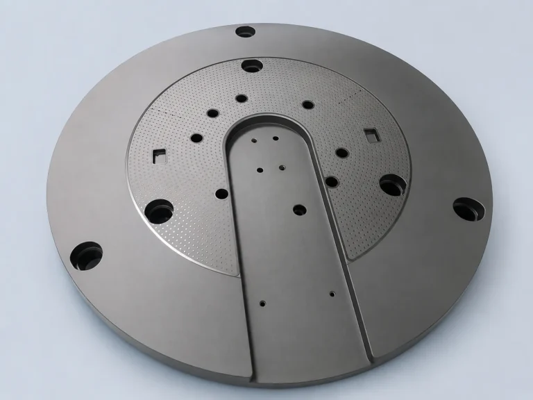
We have extensive experience machining precision metals, engineering plastics, ceramics, glass, fused silica, and other hard and brittle materials. When evaluating semiconductor equipment components, we therefore do not look at CTE alone. Material properties, operating temperature, component geometry, dimensional tolerances, surface requirements, process environment, and actual manufacturability all need to be considered together.
Why Is CTE So Important in Semiconductor Equipment?
The linear dimensional change of a material caused by temperature can be simplified as:
ΔL = α × L × ΔT
where ΔL is the dimensional change, α is the coefficient of linear thermal expansion, L is the original length, and ΔT is the temperature change.
For example, consider a precision structural component with a length of 300 mm and a CTE of approximately 23 ppm/K. If its temperature increases by 10°C, the theoretical dimensional change is approximately 69 μm.
If the same component is made from a low-expansion material with a CTE of approximately 1.2 ppm/K, the dimensional change is only about 3.6 μm.
If a material such as fused silica with a CTE of approximately 0.5 ppm/K is used, the dimensional change may be as low as approximately 1.5 μm.
For general mechanical structures, a difference of 69 μm may not always be critical. For wafer stages, precision metrology systems, optical alignment assemblies, inspection equipment, sensor positioning systems, or precision chucks, however, the difference between tens of microns and only a few microns can represent an entirely different level of system accuracy.
This is why CTE and thermal stability are often key considerations for semiconductor equipment engineers.
Low Thermal Expansion Does Not Automatically Mean the Best Material
Although CTE is important, it should rarely be considered in isolation.
The suitability of a material for a precision semiconductor component also depends on Young’s modulus, thermal conductivity, electrical insulation, vacuum compatibility, outgassing behavior, chemical resistance, plasma resistance, density, wear resistance, fracture toughness, and machinability.
Material price, availability, achievable dimensional tolerance, achievable surface finish, and total manufacturing cost are also important factors.
As a result, the material with the lowest CTE is not necessarily the best material.
For example, if a component requires very low thermal expansion but also needs multiple threaded holes, locating features, countersinks, and complex metallic geometry, Invar may be more practical than glass-ceramics.
If the application requires low CTE together with high stiffness and thermal stability, silicon carbide may be a better choice.
If high thermal conductivity, electrical insulation, and a CTE relatively close to silicon are required, aluminum nitride may offer a better engineering balance.
For optical or high-purity applications, fused silica or low-expansion glass-ceramics may be more suitable.
Engineering plastics such as PEEK, PAI, or polyimide have significantly higher CTE values than Invar or technical ceramics, yet they can still be the better choice when electrical insulation, low weight, chemical resistance, metal-free contact surfaces, or complex CNC geometries are required.
The real objective is therefore not to identify the material with the lowest CTE, but to identify the material that best matches the complete system requirement.
Invar 36: Low Thermal Expansion Without Giving Up Metallic Structure
Invar 36 is one of the most widely recognized low-expansion metals. Its composition consists primarily of iron with approximately 36% nickel, which is why it is also commonly referred to as FeNi36.
The key advantage of Invar is not only its low CTE near room temperature. It also retains the structural and manufacturing characteristics of a metal.
This makes Invar particularly attractive for applications requiring low thermal expansion together with threaded features, precision locating holes, countersinks, thin-wall structures, or complex CNC-machined geometries.
Typical applications may include precision frames, optical mounts, sensor mounts, metrology fixtures, reference structures, precision stage components, high-stability positioning structures, and dimensional inspection fixtures.
Invar, however, also has limitations.
Its relatively high density can become a concern in fast-moving stages or low-inertia positioning systems. Its thermal conductivity is also significantly lower than that of aluminum or copper, meaning that localized temperature gradients can still become a source of dimensional error when the component is positioned close to a continuous heat source.
From a machining perspective, Invar should not be treated in the same way as aluminum.
For high-precision Invar components, machining heat, cutting tool selection, roughing and finishing sequence, residual stress, thin-wall deformation, and final dimensional stability all need to be carefully considered.
We have practical experience in precision Invar machining. When evaluating these components, our focus is therefore not only whether the geometry can be machined, but also whether the final part can maintain the dimensional and geometric stability required by the drawing.
Silicon Carbide: Low Expansion Combined With Exceptional Stiffness
Silicon carbide, or SiC, is an important engineering ceramic used in semiconductor equipment.
Its CTE is generally higher than that of Invar or fused silica, but SiC combines relatively low thermal expansion with a high Young’s modulus, excellent stiffness, high hardness, good thermal conductivity, and strong thermal stability.
For this reason, the value of SiC is not simply that it has a low CTE.
Its real advantage is the combination of low thermal expansion and high structural stiffness.
This makes SiC especially attractive for precision stages, inspection stages, metrology structures, wafer chucks, wafer handling components, pedestals, and other high-stability structural components.
In these applications, it is not enough to minimize dimensional change caused by temperature. The structure must also resist mechanical deflection under its own weight or operating load.
This is one of the reasons SiC can be highly effective in precision semiconductor systems.
Its main disadvantage is manufacturability.
SiC is extremely hard and behaves as a typical hard and brittle material. Precision machining therefore requires careful control of edge chipping, microcracking, thin-wall breakage, small-hole machining, flatness, grinding allowance, and final surface quality.
We have relevant precision machining experience with SiC and other hard and brittle materials. For this reason, manufacturability is often evaluated together with the drawing geometry at an early stage.
For SiC components, design-for-manufacturing considerations are particularly important because a feature that is relatively simple in aluminum or steel may significantly increase machining risk and cost when transferred directly to SiC.
Aluminum Nitride: Not the Lowest CTE, but Often One of the Most Practical Semiconductor Materials
Aluminum nitride, or AlN, is an important ceramic material used in semiconductor equipment, power electronics, and advanced electronic packaging.
If CTE alone is considered, AlN does not have values as low as Invar or fused silica.
Its real advantage is the combination of relatively low thermal expansion, high thermal conductivity, and electrical insulation.
This combination makes AlN especially useful in semiconductor applications.
For ceramic heaters, heater plates, semiconductor chucks, insulating plates, sensor substrates, and high-power semiconductor substrates, components may need to dissipate heat efficiently without becoming electrically conductive.
Under these conditions, AlN provides a highly attractive balance of properties.
Another important advantage is that the CTE of AlN is relatively close to that of silicon.
In semiconductor engineering, the goal is not always to achieve the lowest possible CTE.
In many cases, what matters more is CTE matching.
When silicon is bonded or mechanically integrated with another substrate or structural material, a large difference in thermal expansion can generate thermal stress during repeated heating and cooling cycles.
This may contribute to warpage, bonding stress, delamination, cracking, and reduced long-term reliability.
In these applications, a material with thermal expansion behavior reasonably close to silicon can be more useful than a material with an extremely low CTE.
We also have experience machining precision AlN components. When AlN parts contain small holes, deep holes, narrow grooves, thin walls, localized thin sections, or tight flatness requirements, manufacturing difficulty can increase substantially.
For these materials, it is not enough to determine whether the geometry is technically machinable. The machining method must also be selected to preserve part integrity, dimensional accuracy, and final surface condition.
Silicon Nitride: Low CTE With High Strength and Thermal Shock Resistance
Silicon nitride, or Si₃N₄, is another low-expansion engineering ceramic.
In addition to relatively low thermal expansion, silicon nitride provides excellent mechanical strength, fracture toughness, wear resistance, and thermal shock resistance.
This makes it attractive when a precision component must maintain dimensional stability while also being exposed to mechanical loading or rapid temperature changes.
Compared with some other technical ceramics, silicon nitride offers particularly strong mechanical performance and resistance to cracking.
It may therefore be suitable for precision positioning, wear-resistant, high-temperature, or high-reliability mechanical components.
However, Si₃N₄ remains a hard and brittle material.
Precision small holes, deep holes, complex contours, and very thin geometries can significantly increase machining complexity and cost.
We have practical experience with precision ceramics and other hard and brittle materials, so these parts are typically evaluated from the combined perspective of functionality, geometry, tolerance requirements, and manufacturing risk rather than material properties alone.
Fused Silica: Extremely Low Thermal Expansion for Optical and Precision Applications
Fused silica is one of the most widely recognized ultra-low-expansion materials.
Its CTE is typically around the 0.5 ppm/K level, making it highly resistant to dimensional change caused by temperature.
It also offers high purity, electrical insulation, chemical stability, excellent optical transmission, and low birefringence.
These characteristics make fused silica particularly suitable for optical windows, optical reference components, precision sensor components, photomask-related components, semiconductor optical systems, precision glass substrates, and other thermally stable optical structures.
When the design priority is a combination of extremely low thermal expansion, optical performance, purity, and electrical insulation, fused silica offers clear advantages.
However, it should not be treated as a direct replacement for a metallic structural material.
Fused silica is brittle and relatively sensitive to impact. Holes, slots, thin walls, sharp transitions, and other machined geometries must be designed with edge chipping and microcracking in mind.
If high surface quality is also required, precision grinding or polishing may need to be incorporated into the manufacturing process.
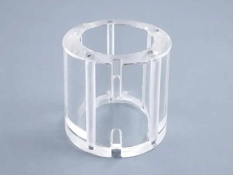
We have precision machining experience with fused silica, quartz, glass, and other hard and brittle materials.
For these components, we typically evaluate drilling, grinding, dimensional machining, surface quality, and edge quality together rather than applying conventional metal CNC machining rules.
ZERODUR and Low-Expansion Glass-Ceramics: When Dimensional Stability Is the Highest Priority
Certain glass-ceramic materials, such as ZERODUR, can achieve thermal expansion extremely close to zero.
For this reason, they are used in high-precision optical systems, metrology references, precision measurement systems, optical stages, and dimensional reference structures where thermal drift must be minimized.
The primary advantage of these materials is exceptional dimensional stability.
The trade-off is typically higher material cost, higher machining cost, longer manufacturing lead time, and lower geometric flexibility compared with conventional metals.
The use of near-zero-CTE glass-ceramics should therefore be justified by actual system requirements.
If a system only requires conventional mechanical tolerances, an expensive ultra-low-expansion glass-ceramic may offer little practical benefit.
If the system must maintain micron-level or even sub-micron geometric stability over changing thermal conditions, however, these materials can become highly valuable.
Alumina and Zirconia: Not the Lowest CTE, but Still Important Semiconductor Ceramics
If materials are ranked only by thermal expansion coefficient, alumina and zirconia will not appear at the top of the list.
However, semiconductor equipment design is not a competition to find the material with the lowest CTE.
Alumina, or Al₂O₃, offers excellent electrical insulation, good wear resistance, good chemical resistance, a mature material supply chain, and relatively manageable cost.
As a result, it remains widely used in ceramic insulators, wafer handling components, ceramic plates, electrical isolation components, and many other semiconductor equipment parts.
We have experience machining precision alumina components, including parts with small holes, grooves, thin walls, precision flat surfaces, and complex ceramic geometries.
This allows machining risk to be considered during the drawing evaluation stage instead of only after material selection has already been finalized.
Zirconia, or ZrO₂, offers a different set of advantages.
Its CTE is not especially low, but it provides high strength, high fracture toughness, excellent wear resistance, and better resistance to cracking than many other technical ceramics.
For parts exposed to contact, impact, wear, or localized mechanical loading, zirconia can sometimes be more appropriate than a lower-CTE but more brittle ceramic.
We also have practical experience machining precision zirconia components, allowing material suitability to be evaluated based on actual geometry, mechanical loading, surface requirements, and operating environment.
Why Are Engineering Plastics Still Widely Used if Their CTE Is Much Higher?
If thermal expansion coefficient is the only consideration, most engineering plastics cannot compete with Invar, fused silica, SiC, or AlN.
Nevertheless, engineering plastics remain widely used in semiconductor equipment because they provide a completely different combination of functional advantages.
Materials such as PEEK, glass-filled PEEK, carbon-filled PEEK, PAI, polyimide, PPS, and PBI can provide electrical insulation, low weight, chemical resistance, and the ability to produce complex CNC-machined geometries.
Certain grades are also suitable for vacuum applications or applications where metal contact should be minimized.
Engineering plastics can also accommodate threaded features, thin walls, grooves, flow channels, and complex three-dimensional geometries that may be difficult or expensive to produce in technical ceramics.
Carbon-filled and glass-filled PEEK can reduce thermal expansion in specific directions while also increasing stiffness.
However, reinforced plastics can exhibit significant anisotropy.
In other words, CTE along the fiber direction may be very different from CTE perpendicular to the fiber direction.
For this reason, engineers should not simply take a single CTE value from a datasheet and use it directly for precision dimensional calculations.
Material grade, fiber content, extrusion direction, machining orientation, operating temperature, glass transition temperature, moisture absorption, and long-term creep should all be considered.
We have precision CNC machining experience with PEEK, PAI, polyimide, and other engineering plastics.
The manufacturing concerns for these materials are very different from those encountered with ceramics. Instead of edge chipping and brittle fracture, the key issues may involve fixturing deformation, machining heat, burr formation, elastic recovery, thin-wall distortion, creep, and long-term dimensional stability.
For this reason, even though engineering plastics do not have the lowest CTE, they may still be the best material choice for specific semiconductor equipment applications.
How Should Semiconductor Engineers Select a Low-Expansion Material?
A practical material selection process should begin with the component’s primary functional requirement.
If extremely low thermal expansion and long-term dimensional stability are the highest priorities, fused silica, ZERODUR, or Invar may be appropriate starting points.
If low CTE must be combined with a metallic structural design, Invar is often highly practical.
If the application also requires high stiffness and thermal stability, SiC or Si₃N₄ may deserve stronger consideration.
If high thermal conductivity and electrical insulation are required simultaneously, AlN may provide greater engineering value than a material with a lower CTE but poorer thermal performance.
For optical applications, fused silica or low-expansion glass-ceramics may be more appropriate.
For electrically insulating components with complex CNC geometries and low weight requirements, PEEK, PAI, or polyimide may be more practical.
These guidelines can help narrow down the initial material options, but final selection should still consider operating temperature, mechanical load, chemical or vacuum environment, component geometry, tolerance requirements, surface quality, and overall manufacturing cost.
Before Selecting the Material, Identify the Real Engineering Problem
The first question should be the actual operating temperature range.
A precision metrology system operating at 20°C ±1°C has very different material requirements from a process chamber component exposed to 200°C or 300°C.
CTE itself also varies with temperature, so room-temperature data should not automatically be assumed to represent behavior over the entire operating range.
The second question is whether the design needs minimum absolute thermal expansion or CTE matching between two different materials.
For an independent precision stage, the lowest possible expansion may be desirable.
For a silicon device bonded to a substrate, heater, or mechanical support, matching the thermal expansion behavior of the materials may be more important than minimizing the CTE of one component alone.
Thermal conductivity should also be considered.
If a component is positioned close to a heater, motor, laser, RF component, or high-power IC, a material with very low CTE but poor thermal conductivity may still experience local temperature gradients and thermal distortion.
This is one reason SiC and AlN are attractive in certain semiconductor systems.
Electrical insulation is another important consideration.
If the component must be both thermally stable and electrically insulating, metallic materials may immediately become unsuitable, and ceramics such as AlN, Si₃N₄, alumina, fused silica, or suitable engineering plastics may need to be considered instead.
Component geometry can also influence material choice.
Deep holes, cross holes, threads, thin walls, narrow slots, undercuts, and complex three-dimensional geometries may be routine in metals but significantly more difficult and expensive in SiC, AlN, or fused silica.
Finally, the actual dimensional requirement should always be reviewed.
If thermal expansion produces only 5 μm of dimensional change while the drawing tolerance is ±0.1 mm, an expensive near-zero-CTE material may not provide meaningful value.
If the system requires ±5 μm, ±2 μm, or sub-micron alignment, thermal stability can become one of the dominant limits on system performance.
Comparison of Common Materials Used in Thermally Stable Semiconductor Components
| Material | Representative CTE | Key Advantages | Main Limitations |
| Invar 36 | Approx. 1 ppm/K range | Ultra-low CTE, metallic structure, CNC machinable | High density, relatively low thermal conductivity |
| Fused Silica | Approx. 0.5 ppm/K | Extremely low CTE, optical performance, high purity, electrical insulation | Brittle, low thermal conductivity |
| Si₃N₄ | Approx. 3 ppm/K range | Low CTE, high strength, good thermal shock resistance | Hard and brittle, high machining cost |
| SiC | Approx. 4 ppm/K range | High stiffness, good thermal conductivity, low CTE | Extremely hard, difficult precision machining |
| AlN | Approx. 4–5 ppm/K | High thermal conductivity, electrical insulation, relatively close CTE to Si | Hard and brittle, relatively high cost |
| Alumina | Approx. 7–8 ppm/K | Electrical insulation, mature supply, wear resistance | Higher CTE than SiC and AlN |
| Zirconia | Approx. 10 ppm/K range | High toughness, high strength, wear resistance | Not considered an ultra-low-CTE material |
| Reinforced PEEK | Depends strongly on grade and direction | Lightweight, insulating, chemical resistant, suitable for complex CNC geometries | Higher CTE, creep, anisotropy |
These values should be used only for preliminary engineering comparison.
Actual thermal expansion coefficients depend on material grade, purity, manufacturing process, fiber orientation, crystal structure, and temperature range.
Final design decisions should always be based on the datasheet for the specific material grade being used.
Excellent Material Properties Do Not Automatically Mean Easy Manufacturing
This is one of the most important considerations in low-CTE material design.
Material selection and manufacturing process should not be treated as two completely separate decisions.
Invar can be conventionally machined, but high-precision parts still require attention to machining heat, residual stress, and the sequence of roughing and finishing operations.
For SiC, AlN, Si₃N₄, alumina, and zirconia, manufacturing concerns shift toward brittle machining, edge chipping, microcracking, thin-wall damage, grinding, and final surface quality.
Fused silica and glass-ceramics require another set of considerations, including edge quality, subsurface damage, dimensional grinding, and polishing.
Engineering plastics such as PEEK, PAI, and polyimide may be easier to machine into complex geometries, but heat generation, fixturing deformation, burr formation, elastic recovery, moisture absorption, and creep can become critical.
A material may therefore look excellent on a datasheet in terms of CTE, modulus, or thermal conductivity, yet still be impractical or unnecessarily expensive when translated into a real component geometry.
A mature engineering decision must consider material performance and manufacturing feasibility together.
From Metals and Engineering Plastics to Ceramics and Hard-Brittle Materials: Why Cross-Material Machining Experience Matters
A semiconductor equipment platform rarely relies on only one material family.
The same system may use Invar for a precision reference structure, aluminum for lightweight mechanical components, stainless steel for vacuum hardware, SiC for wafer handling or structural components, AlN for heater or insulating parts, alumina for electrical isolation, zirconia for wear-resistant features, fused silica for optical components, and PEEK, PAI, or polyimide for precision polymer parts.
Each material performs a different function, and each requires a different manufacturing strategy.
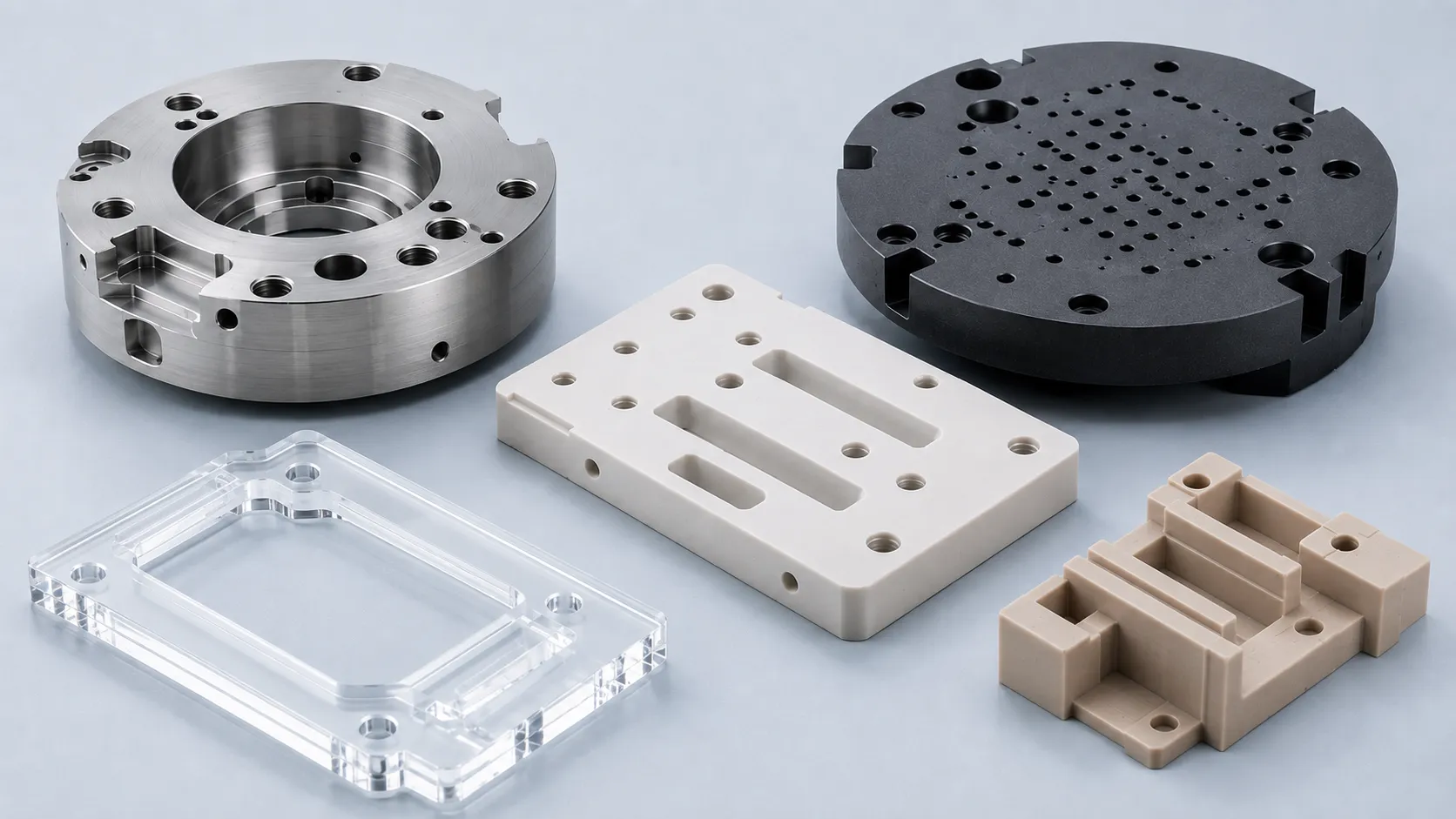
We have extensive machining experience across precision metals, engineering plastics, technical ceramics, quartz, glass, fused silica, and other hard and brittle materials.
This allows us to evaluate semiconductor equipment, wafer handling, precision fixtures, inspection systems, optical systems, and R&D prototype components without being limited to a single material family.
The value of cross-material manufacturing experience is that material selection can remain focused on the component itself.
Operating temperature, thermal cycling, mechanical loading, vacuum or chemical environment, geometry, dimensional tolerance, surface requirements, manufacturing risk, and production cost can all be considered together.
In some applications, Invar may be the best solution.
In others, SiC may provide a better combination of stiffness and thermal stability.
AlN may be the more appropriate material when thermal conductivity and electrical insulation are required simultaneously.
In other cases, an engineering plastic with a higher CTE may still be the better overall choice because it offers lower weight, electrical insulation, chemical resistance, and greater manufacturing flexibility.
For precision semiconductor components, the objective is therefore not to identify the material with the lowest thermal expansion coefficient in the world.
The real objective is to identify the material that offers the best balance of thermal stability, dimensional accuracy, mechanical performance, electrical properties, process compatibility, manufacturability, and total manufacturing cost for the specific component.
That is the real engineering value of low-thermal-expansion material selection.
Engineering Note
The images and examples presented in this article are intended to illustrate common engineering concepts and representative industry practices. To protect customer confidentiality, certain dimensions, geometries, specifications, and application details may have been modified while preserving the underlying engineering principles.