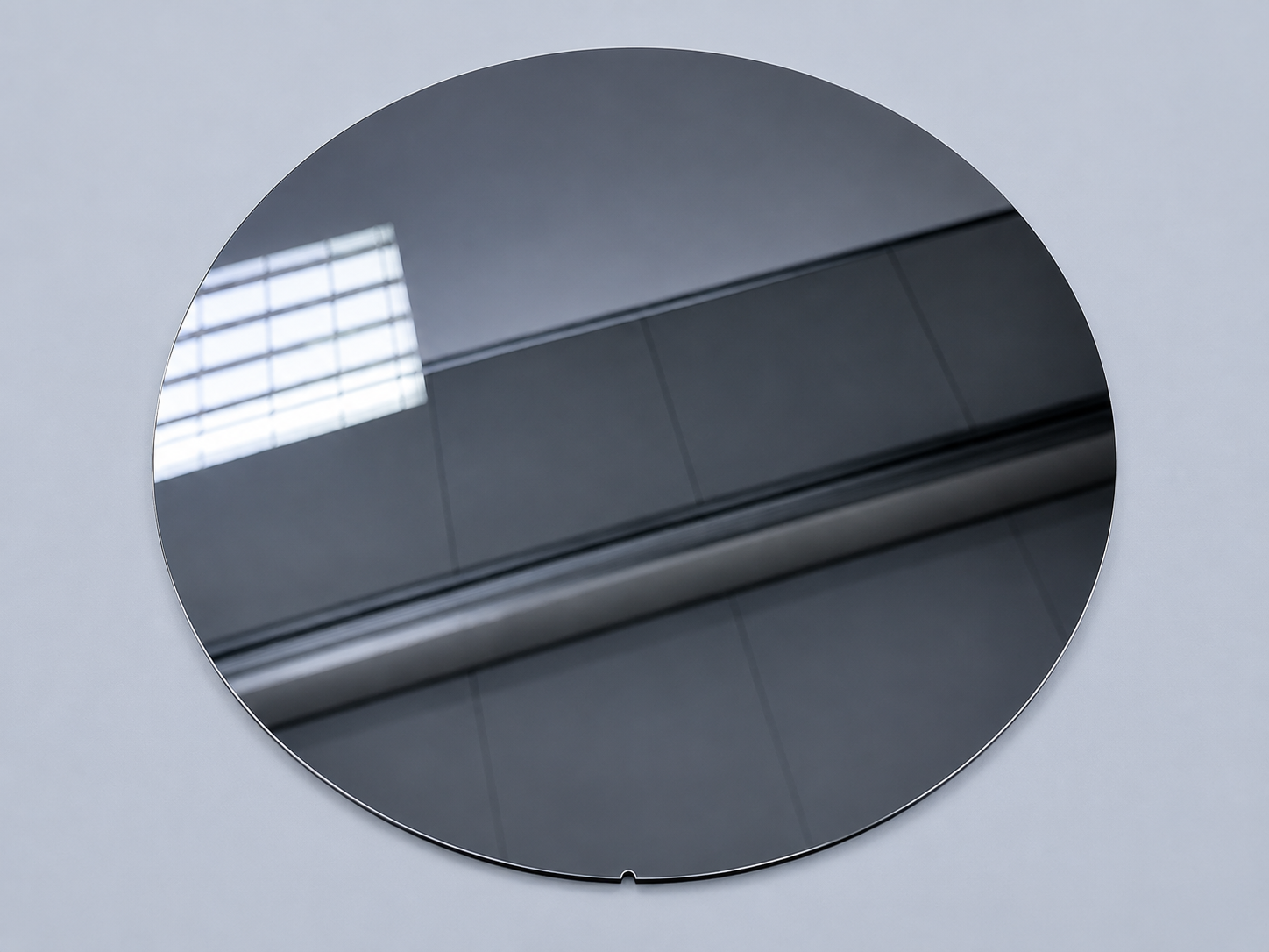
Silicon (Si) is widely used in semiconductor, MEMS, photonics, and optical applications. We machine monocrystalline and polycrystalline silicon into precision wafers, substrates, pocket wafers, and custom components for prototype and low-volume production.
Semiconductor-Grade Material – High-purity silicon for semiconductor, MEMS, and photonics applications.
Low Thermal Expansion – Excellent dimensional stability for precision and vacuum applications.
High Hardness & Stiffness – Supports precision micro-features and high dimensional accuracy.
Excellent Chemical Resistance – Resistant to most chemicals and process environments (except HF).
Precision CNC Machinable – Suitable for wafers, pocket wafers, substrates, and custom components.
Silicon Specifications & Datasheets
We provide precision CNC machining services for semiconductor-grade silicon (Si), including wafers, substrates, pocket wafers, and custom precision components.
A variety of semiconductor-grade silicon materials and custom specifications are available to meet your application requirements.
Trusted by Leading Technology Companies Worldwide
Precision Silicon Machining Capabilities
Challenges & Solutions Silicon is a brittle material that requires specialized machining processes to minimize edge chipping, microcracks, and dimensional variation. Typical Machining Capabilities:
Diamond Grinding – High flatness and parallelism
Pocket Wafer Machining – Precision pockets and recessed features
Micro Slots & Holes – Fine features with minimal edge chipping
Optical Surface Polishing – Mirror-finish surfaces for optical applications
Vacuum Systems – Precision silicon parts for cleanroom and vacuum environments
Research & Laboratory – Custom silicon components for scientific instruments
Post-Processing Options for Silicon
Enhance the performance, surface quality, and functionality of silicon components with our precision post-processing services for semiconductor, MEMS, photonics, and optical applications.
Wafer Back Grinding & Thinning
Precision wafer back grinding and thinning to achieve tight thickness tolerances and excellent flatness for semiconductor applications.
Chemical-Mechanical Polishing (CMP)
Ultra-flat, mirror-quality surfaces with excellent planarity for semiconductor and optical applications.
Silicon Etching
Chemical or plasma etching for surface preparation and semiconductor processing.
Precision Cleaning
Removes particles, machining residues, and surface contaminants to meet semiconductor and cleanroom requirements.
Insulating Thin-Film Coatings
Thin-film dielectric coatings, including thermal oxide, PVD, CVD, and ALD processes, for electrical insulation and semiconductor applications.
Laser Marking
Permanent identification and traceability marking for wafers and precision silicon components.
Additional Ceramics We Support
In addition to Silicon, we offer precision CNC machining services for other hard technical ceramics:
Alumina (Al₂O₃)
Alumina (Al₂O₃) is a durable ceramic used for high-strength, high-temperature parts in precision industries.
Looking for more ceramic machining options? Check out our Capabilities.
Request a Quote for Silicon CNC Machining Today
Looking for high-precision Silicon machining? InstaVoxel delivers expert CNC machining, fast lead times, and superior quality. Contact us today to discuss your project.