
Silicon Carbide Wafer Pin Chuck Machining Case Study for Semiconductor Equipment
In semiconductor equipment, wafer support components are far more than simple mechanical structures. As process accuracy and equipment performance requirements continue to increase, the flatness, stability, surface condition, and dimensional accuracy of the wafer chuck can directly influence wafer positioning, support uniformity, contamination control, and overall process consistency.
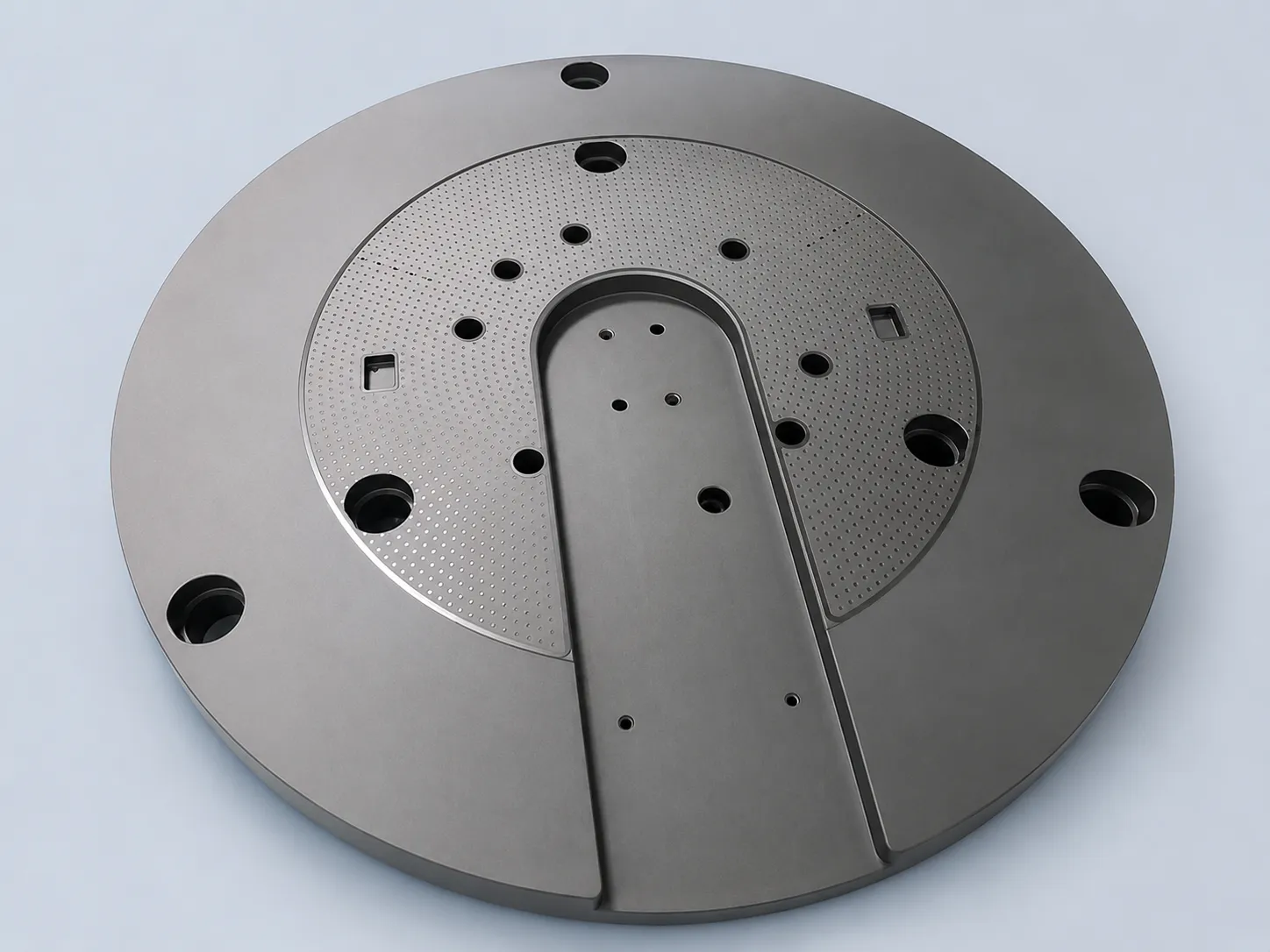
This case study presents a custom silicon carbide wafer pin chuck used in semiconductor equipment. This type of component is also commonly referred to as an SiC pin chuck or bump chuck because its wafer support surface consists of a dense array of precision micro-bumps.
In addition to the micro-bump support area, the component integrates multiple holes, recessed regions, pockets, open sections, and other functional features required for equipment integration.
Although the part may initially appear to be a large circular ceramic plate, its actual manufacturing complexity is considerably higher. The combination of silicon carbide material properties, large-area flatness control, dense micro-feature geometry, functional hole patterns, and precision inspection makes this SiC bump chuck a representative example of high-value precision ceramic machining for semiconductor applications.
What Is a Silicon Carbide Wafer Pin Chuck?
A silicon carbide wafer pin chuck is a precision wafer support component designed to hold a wafer on a large number of small, evenly distributed contact points instead of a continuous flat surface.
Depending on the equipment manufacturer or design, this type of component may also be called a wafer pin chuck, SiC pin chuck, bump chuck, or SiC bump chuck.
The basic design principle is similar: the wafer is supported by a dense array of micro-bumps or short support pins that significantly reduce the actual contact area between the wafer backside and the chuck.
With a conventional flat chuck, a relatively large portion of the wafer backside is in direct contact with the support surface. In a precision semiconductor environment, even small particles or local surface irregularities between the wafer and chuck can create unwanted interference.
A bump chuck reduces the contact area by supporting the wafer on many distributed micro-bumps. This can help improve support consistency while reducing unnecessary backside contact.
Depending on the equipment design, the wafer pin chuck may also operate together with a vacuum system to securely hold the wafer during handling, positioning, inspection, measurement, or other semiconductor processes.
For this reason, wafer pin chucks are especially suitable for applications where wafer stability, repeatability, cleanliness, and precise positioning are important.
Why Silicon Carbide Is Used for Wafer Pin Chucks
Silicon carbide, or SiC, is widely used in high-performance semiconductor equipment because of its excellent combination of mechanical, thermal, and wear-resistant properties.
One of the most important advantages of silicon carbide is its high stiffness. Large wafer chucks and precision stages must maintain their geometry under their own weight, mounting forces, and operating conditions. The high rigidity of SiC helps minimize structural deformation and maintain dimensional stability across the working surface.
Another important characteristic is its relatively low thermal expansion. Semiconductor equipment often operates under tightly controlled conditions where even small temperature variations can affect dimensional accuracy. A material with good thermal stability helps reduce geometry changes caused by temperature fluctuations.
Silicon carbide also provides excellent hardness and wear resistance. For wafer support components that may experience repeated loading and unloading cycles, maintaining the geometry and surface condition of the support area over long-term use is important.
In addition, SiC offers good chemical resistance and overall material stability, making it suitable for demanding semiconductor equipment environments.
For these reasons, silicon carbide is widely considered an excellent material for applications such as:
- Wafer pin chucks
- Bump chucks
- Precision ceramic stages
- Wafer positioning platforms
- Semiconductor structural components
- High-stability ceramic fixtures
Dense Micro-Bump Surface: The Core Feature of the Wafer Pin Chuck
The most distinctive feature of this machining case is the dense micro-bump structure distributed across the wafer support area.
At first glance, these bumps may appear to be simple repeated features. From a manufacturing perspective, however, the real challenge is not simply producing the micro-bumps.
The critical requirement is ensuring that the tops of the individual bumps collectively form a consistent wafer support plane.
If a small number of bumps are higher than the surrounding features, they may create localized high points beneath the wafer. If some bumps are too low, the intended support distribution may also be affected.
For this reason, the performance of an SiC pin chuck depends not only on individual bump dimensions but also on the geometric relationship between all of the support points across the entire chuck.
Important characteristics may include:
- Bump diameter consistency
- Bump pitch accuracy
- Bump height control
- Bump height variation
- Bump coplanarity
- Overall support surface flatness
- Bump top surface condition
- Edge quality
- Chipping control
When hundreds or thousands of micro-bumps are distributed across a large silicon carbide surface, controlling the geometry of one individual bump is only part of the challenge.
The more important objective is maintaining consistent support geometry across the entire wafer contact area.
This is one of the major differences between a precision silicon carbide wafer pin chuck and a conventional machined ceramic plate.
Machining Challenges of a Large SiC Bump Chuck
Silicon carbide is an extremely hard and brittle engineering ceramic. Its machining behavior is significantly different from metals such as aluminum, stainless steel, or titanium.
For a large silicon carbide wafer pin chuck, one of the primary challenges is maintaining flatness across the entire working area.
As component size increases, several manufacturing factors can influence the final geometry, including:
- Workholding conditions
- Grinding forces
- Thermal effects
- Material removal behavior
- Grinding wheel wear
- Process sequence
- Residual geometric variation
Maintaining a precision flat surface on a large SiC component is already challenging. Adding a dense field of micro-bumps significantly increases the complexity.
The bumps must remain geometrically consistent while the brittle silicon carbide material must also be protected from excessive edge chipping, localized damage, or micro-cracking.
Because the support surface directly interfaces with the wafer, even small variations can become important depending on the final equipment application.
For this reason, the quality of a large SiC bump chuck depends on careful control throughout machining, grinding, finishing, and final inspection rather than on any single manufacturing operation.
Integrated Holes, Pockets, and Functional Features
The micro-bump surface is only one part of the overall wafer pin chuck design.
In this case, the silicon carbide component also includes multiple circular holes, recessed regions, open areas, a rectangular pocket, and other customized geometries.
Depending on the equipment architecture, these features may be associated with functions such as:
- Vacuum routing
- Equipment mounting
- Alignment
- Lift pin mechanisms
- Sensors
- Wafer transfer systems
- Mechanical interfaces
- Clearance for moving components
The exact function of each feature depends on the specific semiconductor equipment design.
This means a custom silicon carbide pin chuck should not simply be viewed as a ceramic disk with bumps.
Instead, it is an integrated precision ceramic component combining wafer support, mechanical structure, functional interfaces, and equipment-specific geometry within a single part.
This level of customization is one reason why wafer pin chucks used in advanced semiconductor equipment are typically manufactured according to specific drawings and equipment requirements rather than as standard catalog components.
Typical Manufacturing Process for a Silicon Carbide Wafer Pin Chuck
The exact manufacturing process for an SiC wafer pin chuck depends on the silicon carbide grade, component size, micro-bump geometry, dimensional tolerances, flatness requirements, surface specifications, and final application.
In general, the process may begin with preparation and rough machining of the silicon carbide blank.
The outer geometry, reference surfaces, holes, pockets, recessed areas, and other functional features are then machined according to the component design.
The micro-bump support structure is subsequently formed and refined.
Precision grinding, lapping, and other surface-finishing processes may be used to achieve the required geometry of the wafer support surface and the desired consistency across the bump tops.
After machining and finishing, the component is cleaned and inspected for dimensional accuracy, surface condition, flatness, and other critical characteristics.
For this type of part, the main manufacturing challenge is not simply the sequence of individual operations.
The real challenge is maintaining the required geometric relationships throughout the entire manufacturing process.
Flatness and Bump Coplanarity Are Critical
For a high-precision wafer pin chuck, global flatness and bump coplanarity are among the most important geometric considerations.
A bump chuck contains a large number of individual support points, but these points must function together as one support surface.
If the overall wafer support plane is not sufficiently controlled, the wafer may experience uneven contact or localized loading.
For this reason, dimensional control must consider both local and global geometry.
Depending on the application, important requirements may include:
- Overall chuck flatness
- Bump coplanarity
- Bump height variation
- Parallelism between reference surfaces
- Local surface variation
- Position accuracy of functional features
These requirements are particularly important in semiconductor equipment where wafer positioning, measurement accuracy, alignment, or process repeatability depends on a stable mechanical reference.
Precision Inspection Is as Important as Precision Machining
A high-precision silicon carbide wafer pin chuck cannot always be evaluated using basic dimensional inspection alone.
In addition to measurements such as outside diameter, thickness, hole diameter, and hole position, the functional performance of the chuck may depend on more advanced geometric and surface verification.
Typical inspection characteristics may include:
- Overall flatness
- Parallelism
- Bump height
- Bump height variation
- Bump coplanarity
- Feature position
- Surface roughness
- Local surface variation
Depending on the required precision, inspection may involve high-accuracy CMM systems, optical measurement equipment, profilometry, or other specialized metrology methods.
This combination of precision machining and precision measurement is one of the reasons silicon carbide pin chucks are considered high-value semiconductor equipment components.
The final performance of the part depends not only on the SiC material itself, but also on the ability to control complex geometry, micro-feature consistency, surface condition, and final inspection results.
Applications of Silicon Carbide Wafer Pin Chucks
Silicon carbide wafer pin chucks can be used in a variety of semiconductor equipment platforms where stable wafer support and accurate positioning are required.
Potential applications include:
- Wafer inspection systems
- Wafer metrology equipment
- Precision wafer positioning stages
- Lithography-related equipment
- Laser processing systems
- Wafer handling systems
- Wafer bonding equipment
- Precision measurement platforms
- Advanced semiconductor process equipment
The exact design of the pin chuck can vary significantly depending on wafer size, vacuum configuration, equipment architecture, transfer mechanisms, positioning requirements, and the specific semiconductor process.
For this reason, advanced SiC wafer pin chucks and bump chucks are often highly customized components designed specifically for the equipment in which they will be used.
Precision Silicon Carbide Machining Experience at InstaVoxel
InstaVoxel supports precision machining projects involving silicon carbide and other advanced ceramics for semiconductor equipment and high-precision industrial applications.
Our experience covers a wide range of hard and brittle materials, including:
- Silicon Carbide
- Alumina
- Aluminum Nitride
- Zirconia
- Quartz
- Sapphire
- Other advanced technical ceramics
For custom semiconductor components such as wafer pin chucks, SiC bump chucks, ceramic stages, precision fixtures, structural plates, and advanced ceramic parts, our focus extends beyond basic feature machining.
We also consider the factors that influence actual component performance, including dimensional accuracy, flatness, micro-feature consistency, surface condition, edge quality, and final inspection requirements.
This silicon carbide wafer pin chuck is a representative example.
Although the component appears to be a relatively simple circular ceramic structure, its actual performance depends on the successful integration of material stability, dense micro-bump machining, large-area geometry control, functional feature machining, surface finishing, and precision metrology.
For semiconductor equipment manufacturers, R&D teams, and engineering organizations developing custom wafer handling systems or precision ceramic components, these factors are essential when evaluating the manufacturability and quality requirements of a custom SiC wafer pin chuck.
InstaVoxel provides precision machining support for custom silicon carbide and advanced ceramic components, from prototype development and low-volume production to specialized semiconductor equipment applications.
Engineering Note
The images and examples presented in this article are intended to illustrate common engineering concepts and representative industry practices. To protect customer confidentiality, certain dimensions, geometries, specifications, and application details may have been modified while preserving the underlying engineering principles.