
Porous Ceramic Wafer Grinding Chuck for Wafer Back Grinding and Thinning
In semiconductor wafer back grinding and wafer thinning processes, wafers must remain stable, flat, and uniformly supported while material is removed from the backside. A Porous Ceramic Wafer Grinding Chuck plays a critical role in this process by providing a highly uniform vacuum holding surface for the wafer.
Unlike conventional vacuum fixtures that rely on discrete vacuum holes or grooves, a porous ceramic chuck uses a network of interconnected microscopic pores throughout the ceramic material. Vacuum is distributed across a large surface area, allowing the wafer to be supported more uniformly during grinding.
Because wafer rigidity decreases significantly as the wafer becomes thinner, the performance of the chuck becomes increasingly important. Chuck flatness, vacuum uniformity, surface condition, and dimensional stability can all influence wafer thickness uniformity, Total Thickness Variation (TTV), bow, warp, and overall grinding performance.
Porous ceramic wafer chucks are commonly used in applications including wafer back grinding, wafer thinning, wafer polishing, semiconductor wafer processing, compound semiconductor processing, and precision vacuum holding.
What Is a Porous Ceramic Wafer Grinding Chuck?
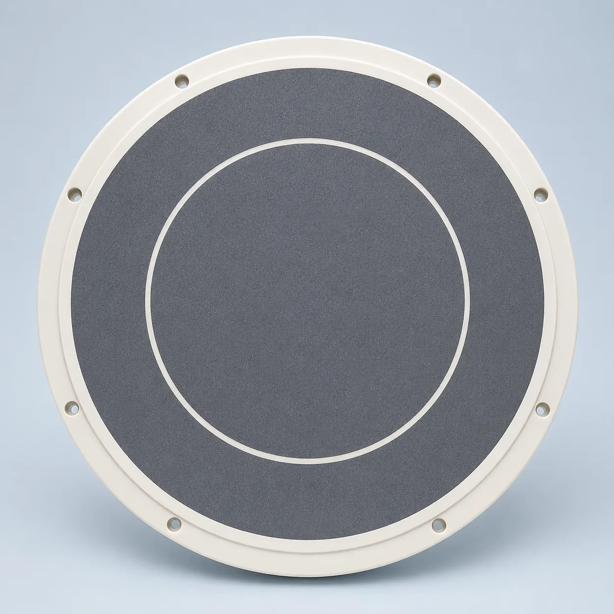
A Porous Ceramic Wafer Grinding Chuck, also referred to as a porous ceramic vacuum chuck or wafer grinding chuck table, is a precision wafer-holding component that uses porous ceramic as the vacuum contact surface.
When vacuum is applied, negative pressure travels through the internal vacuum channels of the chuck and then through the interconnected pores inside the ceramic material. The vacuum is distributed across the porous surface, allowing the wafer to be held securely and relatively uniformly.
This differs from conventional vacuum fixtures, where suction is concentrated around individual holes or grooves. In a porous ceramic chuck, the entire porous area can function as a vacuum transfer surface.
This makes porous ceramic particularly suitable for thin, brittle, fragile, or precision wafers that require uniform support during processing.
Why Is a Porous Ceramic Chuck Important in Wafer Grinding?
In a wafer back grinding process, the front side of the wafer is supported by the chuck while a grinding wheel removes material from the wafer backside.
As the wafer becomes thinner, its mechanical stiffness decreases. This makes it more sensitive to small variations in the supporting surface.
If the chuck has local height variation, uneven vacuum distribution, contamination, clogged pores, or insufficient support, the wafer may deform while being held under vacuum. These effects can ultimately influence the final wafer thickness profile after grinding.
Potential issues may include increased TTV, local over-grinding, wafer bow or warp, edge chipping, cracking, breakage, or abnormal grinding marks.
For this reason, the wafer grinding chuck should not be considered simply a vacuum fixture. It is also an important reference surface within the wafer thinning process.
Typical Structure of a Porous Ceramic Wafer Chuck
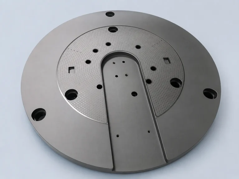
A complete wafer grinding chuck is usually more complex than a single porous ceramic plate. Depending on the equipment and process requirements, it may include a porous ceramic contact surface, a dense supporting base, internal vacuum channels, multiple vacuum zones, mounting features, and sealing structures.
Porous Ceramic Contact Surface
The porous ceramic area is the surface that directly supports the wafer. Its internal pore network allows vacuum to pass through the material and reach the wafer contact surface.
Important characteristics may include pore size, porosity, vacuum flow, vacuum distribution, surface flatness, surface roughness, hardness, and wear resistance.
Pore size must be selected carefully. Larger pores may provide higher flow but can create less uniform surface support, while very small pores may restrict airflow and become more sensitive to contamination or clogging.
Chuck Base and Support Structure
The porous ceramic is typically supported by a dense ceramic, metal, or other high-rigidity base.
The chuck base provides structural stiffness, defines the mounting interface, integrates vacuum channels, and helps maintain the geometric relationship between the wafer contact surface and the machine mounting reference.
Vacuum Channels and Vacuum Zones
Internal vacuum channels distribute negative pressure beneath the porous ceramic.
Some wafer chucks incorporate multiple vacuum zones, such as inner and outer zones, allowing vacuum control to be adapted for different wafer sizes or process conditions.
The design of these internal channels can influence vacuum response, holding force, airflow, and overall vacuum uniformity.
Common Materials for Porous Ceramic Wafer Chucks
Porous Alumina
Porous Alumina (Al₂O₃) is one of the commonly used materials for precision ceramic vacuum chucks.
It offers high hardness, good wear resistance, electrical insulation, chemical stability, and the ability to form controlled porous structures.
These properties make porous alumina suitable for wafer grinding, wafer handling, precision vacuum holding, and other semiconductor equipment applications.
Silicon Carbide
For applications requiring higher stiffness, thermal stability, wear resistance, or thermal conductivity, Silicon Carbide (SiC) may also be considered.
SiC provides high hardness, high rigidity, good thermal conductivity, low thermal expansion, and excellent dimensional stability.
However, the optimum material depends on the equipment configuration, operating environment, vacuum design, cost target, and performance requirement. Not every wafer grinding chuck requires SiC.
Key Technical Requirements
The performance of a wafer grinding chuck cannot be evaluated only by its outside diameter and thickness. The most critical requirements are often related to the wafer contact surface and the geometric relationship between the chuck and the machine.
Flatness
Flatness is one of the most important specifications for a wafer grinding chuck.
If the chuck surface contains local high or low areas, the wafer may deform when vacuum is applied. Even if the grinding wheel follows the machine reference accurately, deformation caused by the chuck can later appear as thickness variation after the wafer is released.
High-precision chucks may therefore require precision grinding, lapping, surface measurement, and dedicated flatness inspection.
The acceptable flatness depends on wafer size, wafer thickness, equipment capability, and process requirements.
Parallelism
Parallelism between the wafer contact surface and the mounting reference is also critical.
A chuck surface may be very flat but still create a thickness gradient if it is not sufficiently parallel to the spindle or equipment reference plane.
For this reason, flatness and parallelism should be considered together.
Surface Roughness
The surface finish of porous ceramic requires a different approach from dense ceramic.
The goal is not simply to produce the lowest possible Ra value. Over-grinding or excessive polishing may modify the pore openings at the surface or partially block the porous structure.
The surface must provide suitable wafer support while maintaining sufficient vacuum transmission.
Porosity and Pore Size
Porosity and pore size influence airflow, holding force, vacuum response, surface support, cleaning behavior, and contamination sensitivity.
Smaller pores can provide more distributed surface support, but may also be more susceptible to clogging. Larger pores can improve flow but may affect local contact characteristics.
The optimum porous structure depends on the wafer, equipment, and process.
Vacuum Uniformity
A wafer chuck should not be evaluated only by whether it can hold a wafer.
Uniformity across the entire working area is equally important.
Local vacuum differences, dead zones, partial clogging, leakage, or uneven internal flow may create different holding conditions across the wafer.
Relationship Between the Chuck and Wafer TTV
TTV, or Total Thickness Variation, is the difference between the maximum and minimum thickness across a wafer.
Many factors can affect TTV, including grinding wheel condition, spindle accuracy, machine alignment, process parameters, wafer condition, and chuck performance.
The chuck contributes because the wafer is ground while held in a constrained condition.
If the chuck surface contains slight geometric errors, the wafer may conform to those errors while vacuum is applied. Once grinding is completed and the wafer is released, the wafer returns toward its free condition, and some of the previous deformation may appear as thickness variation.
The thinner the wafer becomes, the more sensitive it may be to chuck surface accuracy and vacuum distribution.
Therefore, chuck flatness, parallelism, cleanliness, and vacuum uniformity can become increasingly important in advanced wafer thinning applications.
Chuck Dressing and Reconditioning
Porous ceramic wafer chucks are precision equipment components and may experience changes after extended use.
Possible conditions include surface wear, particle contamination, pore clogging, local damage, flatness deviation, and vacuum performance degradation.
Some wafer grinding systems use Chuck Dressing or Chuck Self-Grinding to restore the working surface. A dedicated dressing wheel or grinding wheel is used to correct the chuck surface and recover the required surface condition.
Depending on the condition of the chuck, additional refurbishment options may include cleaning, precision regrinding, lapping, flatness correction, replacement of porous ceramic inserts, or complete chuck reconditioning.
For high-value semiconductor equipment, refurbishment or replacement-part manufacturing may provide an alternative to replacing the complete original assembly.
Wafer Sizes and Typical Applications
Porous ceramic wafer grinding chucks can be designed for common wafer formats such as 4-inch, 6-inch, 8-inch / 200 mm, and 12-inch / 300 mm wafers.
Customized designs may also incorporate special diameters, multiple vacuum zones, non-standard mounting interfaces, custom vacuum channels, or equipment-specific geometry.
In addition to silicon wafers, porous ceramic chucks may also be used for processing other brittle and advanced semiconductor materials, including:
- Silicon Carbide (SiC)
- Sapphire
- Gallium Nitride (GaN)
- Gallium Arsenide (GaAs)
- Glass wafers
- Compound semiconductor wafers
Because these materials differ significantly in stiffness, brittleness, thickness, and grinding behavior, chuck design and vacuum conditions may need to be adjusted for each application.
Manufacturing Challenges of Porous Ceramic Wafer Chucks
Manufacturing a wafer grinding chuck involves much more than machining a ceramic disc.
For large 200 mm or 300 mm chuck assemblies, the manufacturing process must simultaneously control flatness, parallelism, thickness, surface condition, mounting geometry, and vacuum performance.
Porous ceramic is also fundamentally different from dense alumina or dense SiC. Its internal pore structure must remain functional after machining.
Improper machining may lead to surface smearing, pore blockage, edge chipping, local cracking, uneven material removal, or degraded vacuum transmission.
If the chuck uses a composite structure combining porous ceramic with a dense base, additional considerations include bonding accuracy, thermal expansion differences, sealing performance, assembly accuracy, and final surface correction.
Internal vacuum passages also need to be manufactured and connected carefully to maintain airtightness and consistent flow.
After assembly, the final wafer contact surface may require precision grinding and measurement as a complete assembly so that cumulative assembly errors do not affect the final working surface.
Our Manufacturing Experience with Porous Ceramic Wafer Chuck Components
InstaVoxel has experience working with Porous Ceramic Wafer Grinding Chuck components and related precision ceramic vacuum-holding parts for semiconductor applications.
Compared with conventional ceramic components, these parts require attention not only to dimensional machining, but also to porous material behavior, precision surface control, vacuum structure, and the relationship between the porous ceramic area and the supporting base.
In related manufacturing projects, the critical objective is not simply to achieve the required outside diameter, hole positions, or mounting geometry. The working surface that supports the wafer must also be controlled carefully.
During grinding and finishing, porous ceramic requires special attention because improper material removal can affect pore openings, vacuum transmission, surface flatness, and long-term chuck performance.
Depending on the project requirements, manufacturing evaluation may include ceramic machining, precision grinding, flatness and parallelism control, porous surface finishing, vacuum-channel geometry, dimensional inspection, and complete assembly verification.
Replacement Chuck and Reverse Engineering Capability
Many semiconductor tools remain in operation for years, and replacement components for older equipment may become difficult to obtain.
For discontinued, damaged, or custom wafer chucks, replacement-part development may be evaluated using an existing sample, available drawings, 3D models, equipment interface dimensions, or actual process requirements.
A reverse-engineering evaluation may include measurement of the overall geometry, wafer contact area, mounting interface, porous ceramic zone, vacuum inlet positions, sealing features, reference surfaces, and other critical dimensions.
If the internal vacuum structure cannot be directly inspected, additional engineering evaluation may be required before a replacement can be manufactured.
Actual manufacturability always depends on the material, internal configuration, dimensional tolerances, vacuum requirements, and available reference information.
What Information Is Needed for a Custom Wafer Chuck?
For a new, replacement, or custom Porous Ceramic Wafer Grinding Chuck, the following information is useful for engineering evaluation:
- Wafer size
- Chuck outside diameter and thickness
- 2D drawing
- 3D model
- Existing chuck sample
- Porous ceramic material
- Pore size and porosity, if specified
- Flatness requirement
- Parallelism requirement
- Surface roughness requirement
- Vacuum requirement
- Vacuum zone configuration
- Mounting interface
- Operating environment
- Cleaning requirements
- Inspection or documentation requirements
When a complete drawing is not available, an existing chuck sample or equipment interface information may still provide a basis for feasibility evaluation.
Precision Ceramic Manufacturing for Semiconductor Equipment
Porous Ceramic Wafer Grinding Chucks combine several areas of manufacturing technology, including advanced ceramics, precision grinding, vacuum engineering, semiconductor equipment manufacturing, and high-precision metrology.
For this reason, they should not be treated as conventional ceramic CNC components.
Depending on the application, InstaVoxel can evaluate manufacturing requirements for:
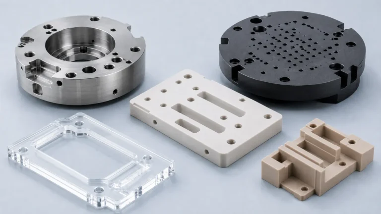
- Precision ceramic machining
- Porous ceramic components
- Alumina and SiC components
- Precision grinding and lapping
- Flatness and parallelism control
- Vacuum chuck components
- Semiconductor equipment replacement parts
- Reverse engineering
- Prototype manufacturing
- Low-volume production
- Dimensional inspection
Each project is evaluated according to the actual material, geometry, tolerance, equipment interface, and process environment.
Why Work with an Experienced Precision Ceramic Manufacturer?
The quality of a wafer chuck depends on more than the machining capability of a single process.
Successful manufacturing requires coordination between material selection, ceramic machining, grinding, assembly, vacuum design, inspection, and final surface control.
For semiconductor equipment manufacturers, R&D teams, wafer-processing facilities, and maintenance organizations, working with a supplier familiar with precision ceramic components can reduce the risk associated with large flat ceramic surfaces, brittle materials, porous structures, and complex replacement-part requirements.
Particular attention should be given to defining the true functional requirements of the chuck rather than only duplicating its visible external geometry.
Conclusion
A Porous Ceramic Wafer Grinding Chuck is a critical precision component in wafer back grinding and wafer thinning equipment.
Its function is not limited to holding the wafer. It also provides the geometric and mechanical support needed to maintain the wafer in a controlled condition during material removal.
Vacuum uniformity, surface flatness, parallelism, porous ceramic quality, dimensional stability, and surface condition can all influence wafer thickness uniformity and overall grinding performance.
As semiconductor manufacturing continues to expand into thinner wafers, 200 mm and 300 mm platforms, SiC, GaN, and other advanced materials, the requirements for wafer chuck accuracy and stability are becoming increasingly demanding.
For custom, prototype, replacement, or legacy-equipment wafer chucks, careful integration of ceramic material selection, precision machining, grinding, vacuum structure, and inspection is essential to achieving reliable performance.
Engineering Note
The images and examples presented in this article are intended to illustrate common engineering concepts and representative industry practices. To protect customer confidentiality, certain dimensions, geometries, specifications, and application details may have been modified while preserving the underlying engineering principles.