

Custom PEEK Feeler Gauge for Semiconductor Equipment – Precision Gap Gauge Case Study
In semiconductor wafer equipment, maintaining precise and repeatable gaps between critical components is essential during assembly, calibration, preventive maintenance, and equipment servicing.
Components such as wafer chucks, heaters, shields, chamber parts, and wafer-handling mechanisms often require specific clearances to ensure proper installation and stable equipment operation.
Standard metal feeler gauges are commonly used for general mechanical gap inspection. However, semiconductor equipment frequently contains narrow spaces, recessed measurement locations, complex surrounding structures, and sensitive surfaces. In these situations, a standard feeler gauge may have the correct thickness but still be unable to reach the required inspection point.
For this reason, a custom semiconductor gap gauge can be designed according to the actual equipment geometry, required measurement thickness, operating environment, and accessibility constraints.
This development case demonstrates a custom PEEK gap gauge with a non-standard thickness of 0.37 ± 0.01 mm, manufactured specifically for semiconductor wafer equipment.
What Is a Semiconductor Gap Gauge?
A gap gauge is a simple but effective inspection tool used to verify the clearance between two components.
Unlike digital measuring instruments or coordinate measuring machines, a gap gauge provides a direct physical method of checking whether a specified clearance has been achieved.
The operator inserts a gauge with a known thickness into the target gap. Depending on the inspection requirement, the gauge can be used to confirm a nominal clearance or determine whether the gap falls within an acceptable range.
Typical semiconductor applications may include:
- Semiconductor equipment assembly
- Wafer processing equipment
- Chamber maintenance
- Wafer chuck and heater installation
- Shield position inspection
- Wafer-handling mechanisms
- Equipment calibration
- Preventive maintenance
- Precision assembly inspection
For applications with defined upper and lower limits, the gauge can also be designed as a GO / NO-GO gap gauge, allowing operators to perform rapid pass/fail inspections without reading a numerical measurement.
Why Are Custom Gap Gauges Needed in Semiconductor Equipment?
Commercial feeler gauges are generally manufactured in standard thicknesses, widths, lengths, and shapes.
These standard products are suitable for many conventional mechanical applications, but semiconductor equipment often presents more complicated inspection conditions.
The required measurement position may be located deep inside a chamber or surrounded by screws, ceramic components, gas-delivery structures, heaters, shields, or other mechanical features.
Even when a commercial feeler gauge is available in a similar thickness, several issues may prevent it from being used effectively:
- The gauge may be too wide to enter the inspection area.
- The blade may not be long enough to reach the target location.
- Nearby components may interfere with the standard blade geometry.
- The handle area may not provide sufficient clearance.
- The required thickness may not be a standard commercially available size.
- Metal contact may be undesirable near sensitive surfaces.
In these situations, the solution is not simply to select another standard gauge.
Instead, the gauge must be designed specifically around the actual equipment structure and inspection method.
Development Case: Custom 0.37 mm PEEK Gap Gauge
In this development case, a customer required a specialized gap gauge for clearance inspection inside semiconductor wafer equipment.
The original inspection method relied on conventional feeler gauges. However, the measurement location was positioned within a restricted area of the equipment, where the surrounding structure prevented a standard gauge from reaching the intended inspection point.
The required measurement thickness was also not a typical standard increment.
The finished measurement section was specified as:
0.37 ± 0.01 mm
In addition to controlling this non-standard thickness, the overall gauge profile had to be customized to fit within the restricted equipment space.
The measurement section was designed to pass around surrounding components and extend into the actual inspection location, while the handling section retained sufficient rigidity for practical use by equipment engineers.
The project therefore involved two key customization requirements:
A non-standard precision thickness and an equipment-specific gauge profile.
This is one of the primary differences between a custom semiconductor gap gauge and a standard commercial feeler gauge. Even if a commercially available product has a similar nominal thickness, it may still be unsuitable because of its fixed geometry or limited accessibility.
Why Was PEEK Selected?
The gauge was manufactured from PEEK (Polyether Ether Ketone), a high-performance engineering thermoplastic widely used in demanding industrial and semiconductor applications.
PEEK offers a balanced combination of:
- Mechanical strength
- Dimensional stability
- Heat resistance
- Wear resistance
- Chemical resistance
- Electrical insulation
- Good machinability for precision components
Compared with a conventional metal feeler gauge, PEEK can also reduce the risk associated with metal-to-surface contact when the inspection location is close to delicate components.
This can be particularly useful around:
- Wafers
- Quartz components
- Technical ceramics
- Coated surfaces
- Precision wafer chucks
- Semiconductor equipment components
PEEK also provides considerably greater rigidity than softer fluoropolymer materials such as PTFE, making it suitable for thin gauges that still require practical handling stiffness.
For these reasons, PEEK is an excellent candidate for custom semiconductor inspection gauges, maintenance jigs, and precision gap-checking tools.
Precision Challenges of a 0.37 mm PEEK Gauge
Although a gap gauge may appear geometrically simple, manufacturing a thin engineering-plastic component with controlled thickness presents several challenges.
At a finished thickness of only 0.37 mm, dimensional consistency becomes significantly more important.
During machining, PEEK can be affected by:
- Material residual stress
- Clamping force
- Cutting heat
- Tool pressure
- Stress release after material removal
- Deformation of thin sections
If only one point of the gauge meets the nominal 0.37 mm thickness while other areas vary significantly, the gauge may no longer provide reliable clearance verification.
For this reason, manufacturing a precision PEEK gap gauge requires attention not only to the nominal dimension, but also to:
- Actual finished thickness
- Thickness consistency across the measurement area
- Flatness
- Warpage control
- Edge quality
- Burr removal
- Dimensional stability of the customized profile
- Surface condition
The machining and fixturing strategy must therefore be selected according to the final thickness, material behavior, and geometry of the gauge.
Alternative Materials for Semiconductor Gap Gauges
PEEK is a highly versatile material for semiconductor inspection gauges, but it is not the only option.
Material selection should depend on operating temperature, chemical exposure, required rigidity, contact surface, cleanliness requirements, and frequency of use.
PEEK
PEEK is suitable for a broad range of semiconductor equipment, wafer-handling, chamber, chuck, heater, and maintenance applications.
Its combination of rigidity, chemical resistance, wear resistance, and dimensional stability makes it a strong general-purpose choice.
PTFE
PTFE offers excellent chemical resistance and very low friction.
It may be suitable for applications associated with:
- Wet processing
- Chemical cleaning
- Etching
- Acid or alkaline environments
However, PTFE is significantly softer than PEEK. Thin or elongated gauges therefore require careful evaluation of rigidity and dimensional stability.
PI – Polyimide
Polyimide is suitable for applications requiring higher temperature resistance.
It can be considered for semiconductor inspection tools and jigs operating under thermal conditions where conventional engineering plastics may become unsuitable.
PAI – Polyamide-Imide
PAI, including materials such as Torlon®, offers high mechanical strength, rigidity, wear resistance, and excellent performance at elevated temperatures.
It can be considered for inspection gauges requiring higher dimensional stability, repeated use, or demanding thermal conditions.
The final material should therefore be selected according to the actual process environment rather than using a single material for every application.
Custom Shapes for Wafer Equipment Inspection
Semiconductor equipment varies significantly in internal layout, making standardized gap-gauge geometry unsuitable for many applications.
Custom gauges can be manufactured according to customer-provided 2D drawings, CAD models, or actual inspection conditions.
Possible configurations include:
- Non-standard thickness gap gauges
- Ultra-thin PEEK gauges
- Narrow-tip gauges
- Locally reduced-width designs
- Clearance profiles
- L-shaped gauges
- T-shaped gauges
- Step gauges
- Extended-handle gauges
- Custom inspection profiles
- GO / NO-GO gauges
- Laser-marked part numbers
- Laser-marked thickness identification
This type of customization is particularly suitable for prototype equipment, R&D systems, special semiconductor tools, and low-volume maintenance applications where commercially available gauges cannot meet the inspection requirement.
Custom GO / NO-GO Gap Gauges
A custom gap gauge can also be designed as a GO / NO-GO inspection tool when a specific clearance range must be maintained.
For example, two different thicknesses can be incorporated into a single inspection gauge.
The operator can quickly confirm that:
The GO section enters the gap, while the NO-GO section does not.
This allows a quick pass/fail decision without repeatedly changing between several individual feeler gauges.
Custom GO / NO-GO gauges can be particularly useful for:
- Preventive maintenance
- Equipment assembly
- Repetitive machine inspection
- Standardized maintenance procedures
- Production equipment verification
They can also help reduce inspection variation between different operators.
From a Standard Feeler Gauge to an Equipment-Specific Inspection Tool
The value of a custom semiconductor gap gauge is not simply the ability to machine a piece of PEEK to a specified thickness.
The real objective is to convert the customer’s:
target gap, equipment geometry, measurement position, insertion method, operating environment, and accessibility limitations
into a practical inspection tool that can be used repeatedly and consistently by equipment engineers.
When the inspection location involves restricted access, non-standard thickness, complex geometry, or sensitive components, a standard commercial feeler gauge may not provide an effective solution.
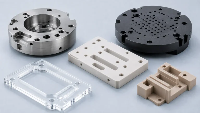
Through precision machining, semiconductor gap gauges can be customized in PEEK, PTFE, PI, PAI, or other high-performance engineering plastics according to the actual equipment requirements.
For prototype, R&D, special wafer equipment, and low-volume maintenance applications, custom manufacturing provides an effective alternative to fixed-size commercial gauges.
Engineering Note
The images and examples presented in this article are intended to illustrate common engineering concepts and representative industry practices. To protect customer confidentiality, certain dimensions, geometries, specifications, and application details may have been modified while preserving the underlying engineering principles.