
Precision Machined BGA IC Test Socket Components for Semiconductor Testing
As semiconductor devices continue to increase in pin count, computing performance, and signal speed, BGA (Ball Grid Array) packages are becoming increasingly dense and complex. High-performance devices such as ASICs, FPGAs, CPUs, GPUs, AI accelerators, and other advanced integrated circuits may contain hundreds or even thousands of electrical contact points within a relatively small package area.
Before these devices are delivered or integrated into electronic systems, they typically undergo electrical testing to verify functionality and performance. An IC Test Socket serves as the temporary mechanical and electrical interface between the semiconductor device and the testing system.
Although an IC Test Socket may appear to be a relatively simple mechanical fixture, its internal components often require extremely accurate machining, especially when dealing with high-density BGA packages and fine-pitch probe arrays.
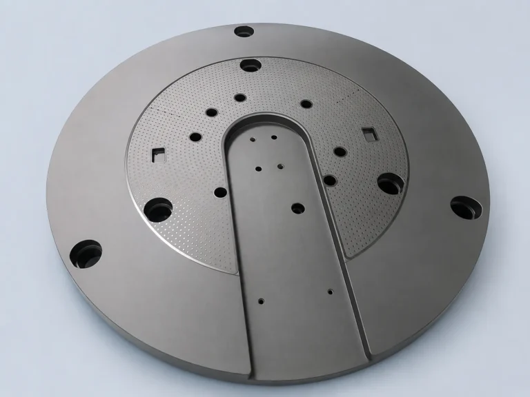
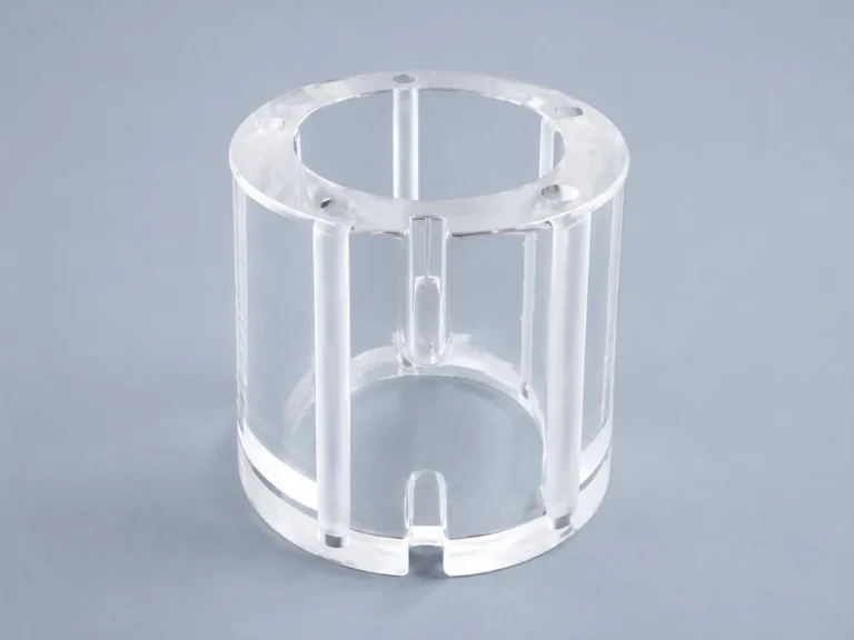
Our team has machining experience with precision components related to IC Test Socket assemblies, including structures featuring high-density hole arrays, precision positioning features, and tight dimensional relationships. These projects require not only accurate machining of individual features, but also careful control of the entire array geometry and assembly references.
What Is an IC Test Socket?
An IC Test Socket is a precision fixture used to temporarily hold a semiconductor device while establishing electrical contact between the IC and automated test equipment.
Unlike soldering an IC directly onto a PCB, a Test Socket allows the device to be repeatedly inserted, tested, and removed.
A typical semiconductor test configuration can be represented as:
IC / BGA Device
→ IC Test Socket
→ Load Board or DUT Board
→ ATE Semiconductor Tester
ATE refers to Automatic Test Equipment, while DUT means Device Under Test.
When the IC is inserted into the socket, a mechanical compression system applies a controlled force. This allows the BGA balls or contact pads on the device to make contact with spring probes, pogo pins, elastomer contacts, or other electrical contact structures inside the socket.
The signals then pass through the Load Board to the semiconductor testing equipment.
Applications of BGA IC Test Sockets
IC Test Sockets are widely used throughout semiconductor development and production.
One common application is Final Test, where packaged semiconductor devices are electrically tested before shipment. Test Sockets are also frequently used during Engineering Test and Characterization Test, where engineers evaluate device behavior under different voltage, frequency, temperature, and operating conditions.
They may also be used in Burn-in Testing and reliability evaluation, particularly when devices must operate for extended periods under elevated temperatures or electrical loads.
For semiconductor R&D and Failure Analysis, removable socket systems are especially useful because the same test setup can accommodate repeated installation and removal of different IC samples.
High-Density Probe Guides in BGA Test Sockets
One of the most important precision components within many BGA Test Socket designs is the Probe Guide.
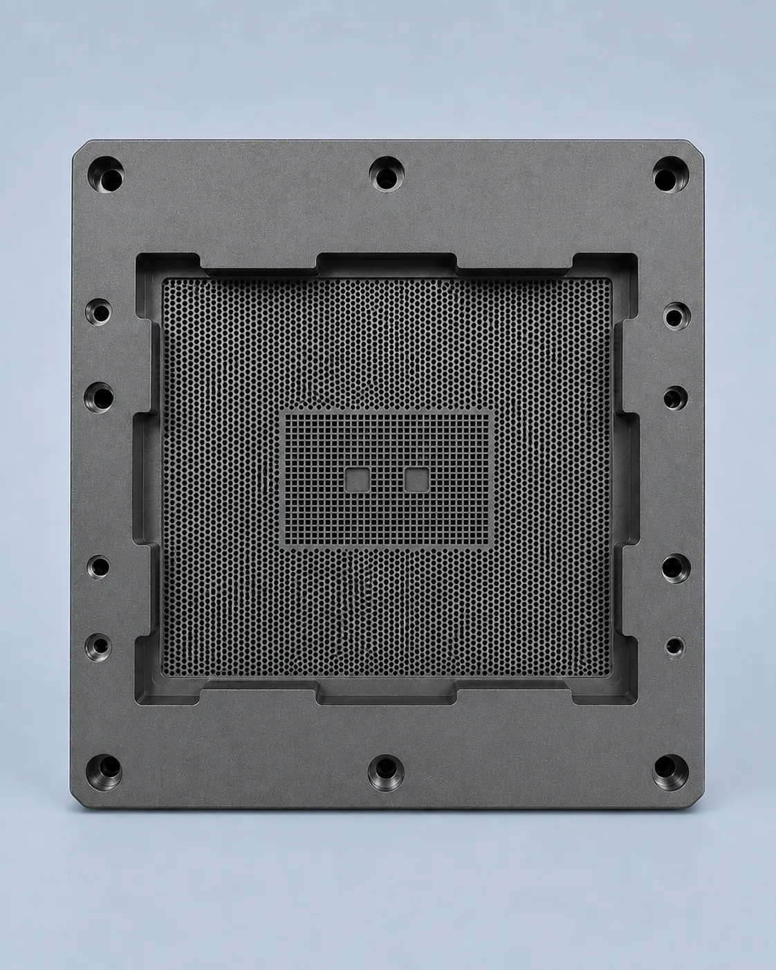
A Probe Guide may contain hundreds or thousands of small holes arranged in a highly accurate grid pattern. Each hole corresponds to a specific electrical contact position on the BGA package.
Depending on the socket design, these holes may guide spring-loaded probes or other contact elements that connect the IC to the Load Board.
For a high-pin-count BGA package, the Probe Guide therefore becomes much more than a plate with many drilled holes.
The diameter, pitch, position, straightness, and overall array accuracy can directly influence probe alignment and contact reliability.
This is why machining a high-density Probe Guide should be considered a precision array machining process rather than simply a repetitive drilling operation.
Why Machining Accuracy Is Critical
Modern BGA packages may use pitches such as 0.80 mm, 0.65 mm, 0.50 mm, or even smaller depending on the device and packaging technology.
As the pitch decreases, the allowable positional variation between the BGA contact and the corresponding probe also becomes smaller.
A high-density Test Socket component therefore requires control over several machining factors at the same time.
Micro-Hole Diameter and Position
The hole diameter must match the probe structure being used.
If a guide hole is too small, the probe may not move freely. If the hole is too large, excessive clearance may reduce guidance accuracy and affect probe alignment.
However, hole diameter alone is not enough.
The positional relationship between each hole, the overall hole array, the IC locating features, and the assembly datums must also be controlled.
For this reason, true position and array alignment can be more important than simply maintaining an individual hole diameter tolerance.
Controlling Accumulated Pitch Error
Pitch accumulation is another critical consideration in high-density BGA components.
For example, if a Probe Guide uses a 0.50 mm pitch and contains approximately 100 positions across one direction, the entire array spans nearly 50 mm.
Even very small deviations between adjacent holes can become significant when accumulated across a large array.
Therefore, machining control may involve more than conventional ± dimensional tolerances.
Important characteristics can include:
- Hole-to-hole pitch consistency
- Overall array position
- Datum-to-array relationship
- Pattern alignment
- X-Y dimensional stability
- Local and global positional accuracy
Maintaining these relationships across hundreds or thousands of features is one of the main challenges in manufacturing high-density Test Socket components.
Flatness and Thickness Control
Electrical contact reliability is not determined only by X-Y positioning.
The Z-axis geometry of the component is equally important.
If the Probe Guide, alignment plate, or support structure has insufficient flatness, some areas of the IC may engage the probes before others. This can result in non-uniform probe compression and inconsistent contact force across the package.
For devices containing thousands of contact points, even relatively small variations in flatness or thickness may influence the consistency of the test interface.
As a result, important machining parameters may include:
- Flatness
- Parallelism
- Overall thickness
- Local thickness consistency
- Assembly height
These requirements become especially important for large BGA packages and fine-pitch test interfaces.
Burr Control and Micro-Hole Quality
Burrs, debris, edge deformation, and damaged micro-hole entrances can interfere with probe installation and movement.
The machining strategy therefore needs to consider not only dimensional accuracy but also the quality of each hole.
Engineering plastics may develop burrs, local deformation, or thermal damage if inappropriate cutting conditions are used.
Ceramic materials present a different challenge. Because ceramics are hard and brittle, micro-hole machining may involve risks such as edge chipping, cracking, and local fracture.
Tool selection, machining sequence, material support, cutting parameters, and final cleaning are therefore important aspects of producing reliable Probe Guide components.
Common Materials for IC Test Socket Components
Material selection depends on test temperature, electrical requirements, mechanical loading, dimensional stability, signal characteristics, and the structure of the Test Socket.
Common materials include high-performance engineering plastics, ceramics, and metals.
PEEK
PEEK offers a useful combination of mechanical strength, thermal resistance, chemical resistance, electrical insulation, and dimensional stability.
It is widely used in semiconductor equipment and precision fixtures and can be suitable for various socket insulators, positioning components, and guide structures.
Torlon PAI
Torlon PAI provides excellent mechanical strength, rigidity, and dimensional stability at elevated temperatures.
For precision parts requiring higher stiffness and resistance to deformation, Torlon can be an attractive material option.
Vespel PI
Vespel polyimide materials are known for their high-temperature capability, dimensional stability, and performance in demanding semiconductor and vacuum environments.
Certain Test Socket or probe-related components may use Vespel when thermal and mechanical requirements justify its higher material cost.
PEI and PPS
PEI and PPS can also be considered for electrical insulation and precision mechanical structures depending on operating temperature, cost, dimensional requirements, and application conditions.
Precision Ceramics
Alumina and other technical ceramics provide excellent electrical insulation, hardness, thermal resistance, and dimensional stability.
For specific high-temperature or highly stable probe guide applications, ceramic components may provide advantages over engineering plastics.
However, machining ceramics requires specialized processes because of their hardness and brittleness.
Aluminum and Stainless Steel
Metallic materials are commonly used for Socket Housings, Frames, Retainers, and structural components.
Aluminum provides low weight and good machinability, while stainless steel may be selected when higher strength, wear resistance, or structural rigidity is required.
A complete IC Test Socket can therefore combine several different material families within a single assembly.
Precision Components Within an IC Test Socket Assembly
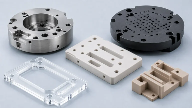
From a precision machining perspective, an IC Test Socket may include several custom mechanical components, such as:
- Probe Guide
- IC Alignment Plate
- Socket Housing
- Insulator
- Spacer
- Retainer
- Compression Plate
- Precision Frame
- Custom locating components
Different components have different manufacturing priorities.
Probe Guides and Alignment Plates typically emphasize micro-hole accuracy, pattern positioning, and dimensional stability.
Socket Housings and Frames focus more heavily on assembly datums, rigidity, mounting interfaces, and accurate relationships between multiple features.
For this reason, manufacturing an IC Test Socket assembly often requires experience with multiple materials and different machining strategies.
Our Experience With Test Socket Related Precision Machining
We have experience machining precision components related to semiconductor IC Test Socket applications.
These components can involve dense micro-hole patterns, precision reference surfaces, positioning features, and close relationships between the hole array and surrounding mechanical structures.
In these projects, one of the most important considerations is maintaining consistency across the complete component.
Producing one accurate hole may not be particularly difficult. Producing hundreds or thousands of holes while maintaining the required pitch, position, flatness, and dimensional stability across the entire part is significantly more challenging.
Our machining approach considers factors such as material behavior, machining sequence, tooling condition, thermal deformation, workholding, datum control, and inspection requirements.
For prototype and low-volume semiconductor applications, this flexibility is particularly valuable because Test Socket components are often customized for a specific IC package rather than produced as standard off-the-shelf mechanical parts.
Our machining capability focuses on the precision mechanical components used within the Test Socket assembly. Electrical contact design, probe selection, signal integrity, and complete ATE system design are typically determined by the Test Socket designer or semiconductor testing equipment manufacturer.
Prototype and Custom BGA Test Socket Components
Semiconductor R&D frequently requires Test Sockets for devices that are still under development.
In these situations, production quantities may initially be very small, while dimensional and functional requirements remain demanding.
Custom machining is therefore particularly suitable for:
- Engineering samples
- Prototype Test Sockets
- New BGA package development
- Custom Probe Guides
- Low-volume semiconductor testing fixtures
- Replacement socket components
- Modified IC positioning structures
- Special high-temperature testing applications
Manufacturing methods and materials can be selected according to the drawing, 3D model, hole pattern, pitch, tolerance, test environment, and required quantity.
What Should Be Evaluated Before Manufacturing a Probe Guide?
When evaluating a high-density Probe Guide, the smallest hole diameter is only one part of the manufacturing challenge.
Other information should also be reviewed, including:
- Material
- Hole diameter
- Number of holes
- Hole depth
- Hole pitch
- Array dimensions
- Positional tolerance
- Flatness
- Part thickness
- Datum structure
- Surface requirements
- Operating temperature
- Quantity
For example, machining twenty Ø0.30 mm holes is completely different from producing three thousand Ø0.30 mm holes in a precision array.
The latter requires careful consideration of tool life, machining time, thermal stability, workpiece deformation, accumulated positioning error, and inspection strategy.
Conclusion
The IC Test Socket is an important interface between packaged semiconductor devices and Automatic Test Equipment.
As BGA packages continue toward higher pin counts, smaller pitches, and more demanding electrical performance, the mechanical precision of Test Socket components becomes increasingly important.
For Probe Guides, IC Alignment Plates, Socket Housings, and related precision parts, the manufacturing challenge is not simply producing a large number of holes.
The key challenge is maintaining consistent hole diameter, pitch, position, flatness, thickness, and overall dimensional accuracy across the complete component.
Materials such as PEEK, Torlon PAI, Vespel PI, PEI, PPS, technical ceramics, aluminum, and stainless steel can each provide different advantages depending on the testing environment and mechanical requirements.
With experience in precision machining of Test Socket related components and semiconductor-grade engineering materials, we can support customized prototype and low-volume components based on customer drawings, 3D models, material requirements, and dimensional specifications.
Engineering Note
The images and examples presented in this article are intended to illustrate common engineering concepts and representative industry practices. To protect customer confidentiality, certain dimensions, geometries, specifications, and application details may have been modified while preserving the underlying engineering principles.