
Wafer Thinning / Back Grinding: Key Technologies Behind High-Precision Semiconductor Wafer Processing
As advanced packaging, MEMS, optical sensors, 3D ICs, and power semiconductor technologies continue to evolve, Wafer Thinning and Back Grinding have become essential processes in modern semiconductor manufacturing.
From standard 725 µm silicon wafers to today’s ultra-thin wafers used in high-density packaging and sensor applications, wafer processing is no longer just about material removal. The real challenge lies in reducing wafer thickness while maintaining flatness, minimizing chipping, controlling particle contamination, and protecting delicate front-side circuitry and microstructures.
For many high-precision and R&D-oriented applications, wafer thinning also involves:
- Ultra-thin wafer handling
- Front-side circuit protection
- Cleanliness and particle control
- Low-warp processing
- Special cavity or pocket wafer structures
- Integration with coating and inspection processes
This is what differentiates advanced wafer processing from conventional grinding operations.
What is Wafer Thinning?
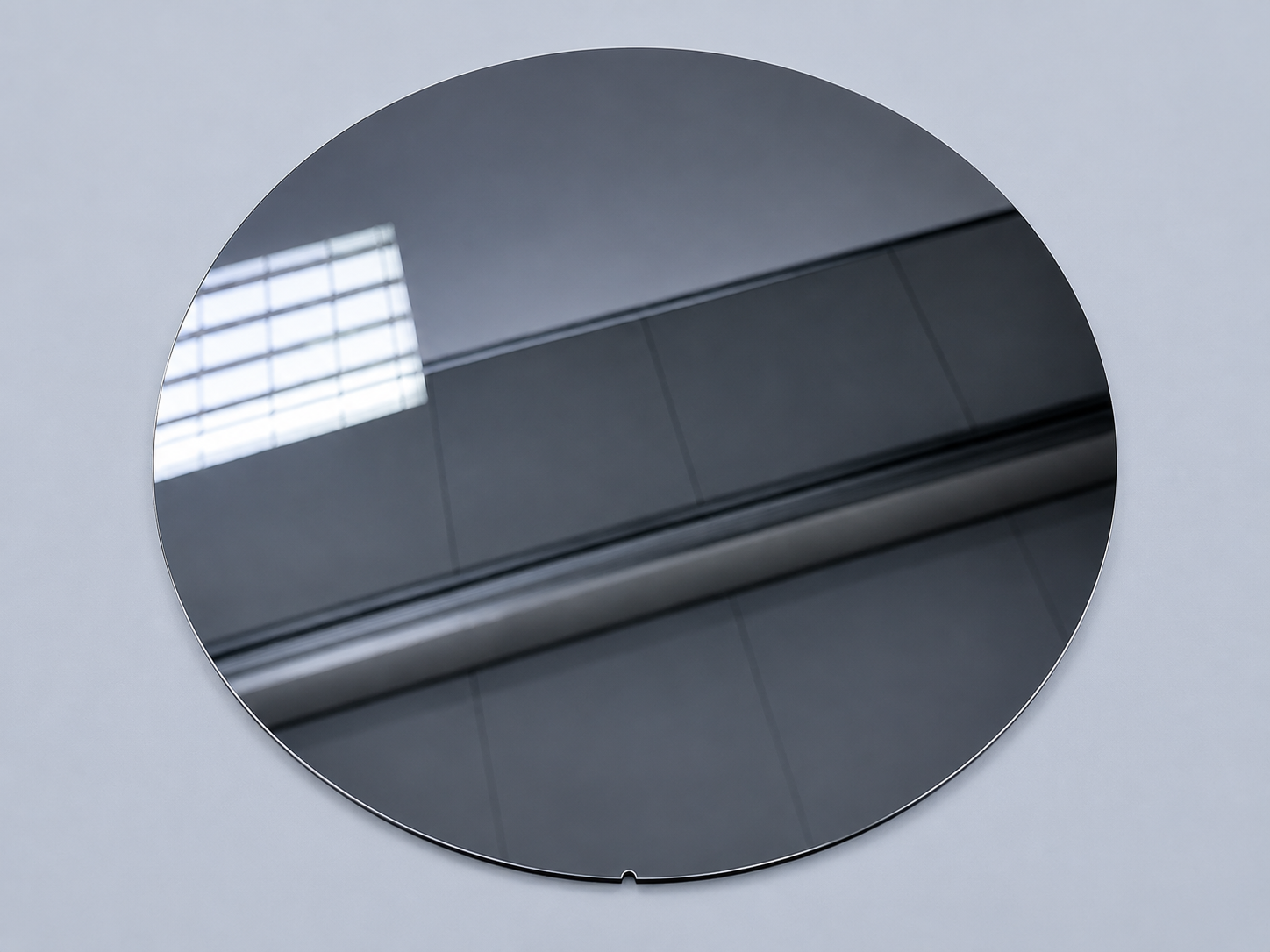
Wafer thinning is the process of reducing wafer thickness through methods such as back grinding, CMP (Chemical Mechanical Polishing), etching, or precision polishing.
Thinned wafers are widely used in:
- Advanced packaging
- TSV (Through Silicon Via)
- MEMS devices
- Optical sensors
- CIS image sensors
- SiC and GaN power devices
- High-density electronic modules
Typical Wafer Thickness by Wafer Size
Typical semiconductor wafer thickness varies depending on wafer diameter and application requirements.
| Wafer Size | Typical Standard Thickness |
| 200 mm (8-inch) silicon wafer | Approx. 725 µm |
| 300 mm (12-inch) silicon wafer | Approx. 775 µm |
After wafer thinning / back grinding processes, typical final thickness ranges may include:
| Application | Typical Final Thickness |
| General wafer thinning | 300–500 µm |
| Advanced packaging | 100–300 µm |
| Ultra-thin wafer applications | <100 µm |
As wafer thickness decreases, the material becomes increasingly fragile and more sensitive to stress, warpage, and handling damage, requiring highly controlled processing conditions.
What is Back Grinding?
Back Grinding is one of the most common wafer thinning methods, using precision grinding equipment to remove material from the backside of the wafer.
A typical process flow includes:
- Front-side protection
- BG tape mounting
- Coarse grinding
- Fine grinding
- Stress relief processing
- Cleaning
- Final inspection or coating
Among these steps, one of the most critical — yet often overlooked — is front-side protection.
Why Front-Side Protection is Critical During Wafer Thinning
The front side of a wafer often already contains:
- IC circuitry
- Metal layers
- MEMS structures
- Fine patterns
- Optical structures
- Sensor components
Without proper protection, the grinding process can cause:
- Surface scratches
- Pattern damage
- Metal layer failure
- Particle contamination
- Wafer cracking
- Micro-cracks
For this reason, front-side protection is typically required before back grinding begins.
Common Front-Side Protection Methods
BG Tape (Back Grinding Tape)
The most widely used method involves applying specialized protective tape to the front side of the wafer.
BG tape helps:
- Protect delicate circuitry
- Reduce grinding stress impact
- Prevent particle adhesion
- Provide mechanical support
- Lower wafer breakage risk
Different wafer structures and surface conditions often require different tape materials and adhesive properties.
Temporary Bonding / Carrier Wafer Support
For ultra-thin wafers, BG tape alone may not provide sufficient mechanical stability.
In these cases, wafers are temporarily bonded to:
- Glass carriers
- Silicon carriers
- Temporary adhesive bonding systems
before thinning operations begin.
This approach is commonly used for:
- Ultra-thin wafers
- MEMS wafers
- TSV applications
- Pocket wafers
- High-precision sensor wafers
Common Challenges in Wafer Thinning
Wafer Warp and Bow
As wafers become thinner, they become increasingly sensitive to residual stress.
Excessive warp can affect:
- Robotic handling
- Vacuum chuck stability
- Lithography alignment
- Packaging yield
Stress management and optimized grinding conditions are therefore essential.
Edge Chipping
Silicon and many wafer materials are inherently brittle.
Improper grinding parameters can lead to:
- Edge chipping
- Micro-cracks
- Crack propagation
This becomes even more critical for ultra-thin wafers.
Particle Control
In semiconductor and optical applications, particle control is often even more important than dimensional tolerance.
Advanced wafer processing typically involves:
- RCA cleaning
- Megasonic cleaning
- Ultra-pure DI water
- Cleanroom handling
to minimize contamination risks.
TTV (Total Thickness Variation)
TTV measures wafer thickness uniformity.
High-precision applications often require:
- Extremely low thickness variation
- Excellent flatness
- Stable surface quality
These factors directly impact downstream packaging and process yield.
Industries That Require Wafer Thinning
Wafer thinning is widely used across multiple industries.
Advanced Semiconductor Packaging
Applications include:
- 2.5D / 3D IC
- Fan-Out Packaging
- TSV integration
MEMS and Sensor Devices
Examples include:
- Pressure sensors
- Microfluidic devices
- Accelerometers
Optical and Photonics Applications
Examples include:
- CIS image sensors
- Photonics devices
- LiDAR systems
- Optical inspection systems
Power Semiconductor Applications
Examples include:
- SiC wafers
- GaN wafers
Wafer thinning can improve:
- Thermal dissipation
- Packaging efficiency
- Electrical performance
Advanced Wafer Processing is More Than Just Grinding
Wafer thinning is often misunderstood as a simple grinding operation. In reality, high-end wafer processing requires expertise in:
- Ultra-thin wafer handling
- Front-side protection
- Stress management
- Particle control
- Cleanroom packaging
- Wafer geometry control
- Process integration
Especially for prototype wafers, pocket wafers, cavity wafers, and optical applications, successful projects often require integration of:
- Precision machining
- Wafer cleaning
- Coating processes
- Inspection and metrology
- Clean handling procedures
InstaVoxel Wafer Processing Capabilities
InstaVoxel Official Website
InstaVoxel provides high-precision wafer processing and custom engineering solutions for semiconductor, photonics, and advanced technology applications.
Our capabilities include:
- Wafer Thinning
- Back Grinding
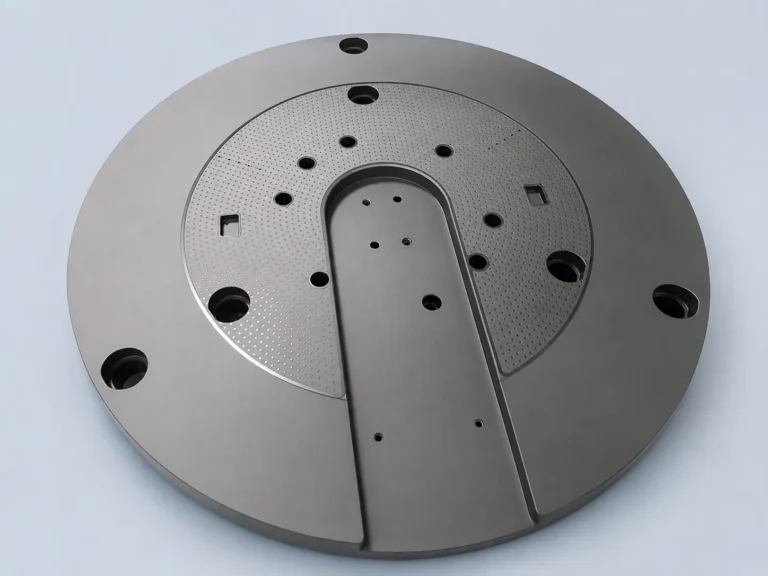
- Pocket Wafer Machining
- Cavity Wafer Processing
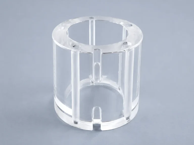
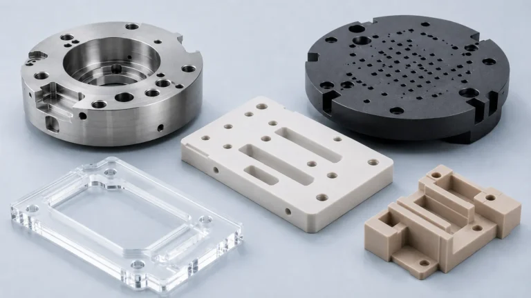
- Advanced Material Machining
- Precision Inspection Integration
We specialize in:
- Brittle material machining
- Low-volume R&D wafer projects
- Clean handling procedures
- Complex wafer geometries
- Precision metrology integration
We also support integrated engineering workflows including:
- Cleaning
- Thin-film processing
- Surface treatment
- Precision inspection
- Custom wafer engineering services
Conclusion
As advanced packaging, MEMS, and photonics technologies continue to evolve, wafer thinning and back grinding have become highly integrated precision engineering processes rather than simple material removal operations.
From front-side circuit protection and ultra-thin wafer handling to particle control and thickness management, every detail directly impacts product quality and manufacturing yield.
For high-end wafer applications, choosing a manufacturing partner with expertise in precision machining, clean handling, and wafer engineering can make a significant difference in project success.
Engineering Note
The images and examples presented in this article are intended to illustrate common engineering concepts and representative industry practices. To protect customer confidentiality, certain dimensions, geometries, specifications, and application details may have been modified while preserving the underlying engineering principles.