
Insulation Layer Process Analysis for Pocket Wafers and High Aspect Ratio Semiconductor Structures
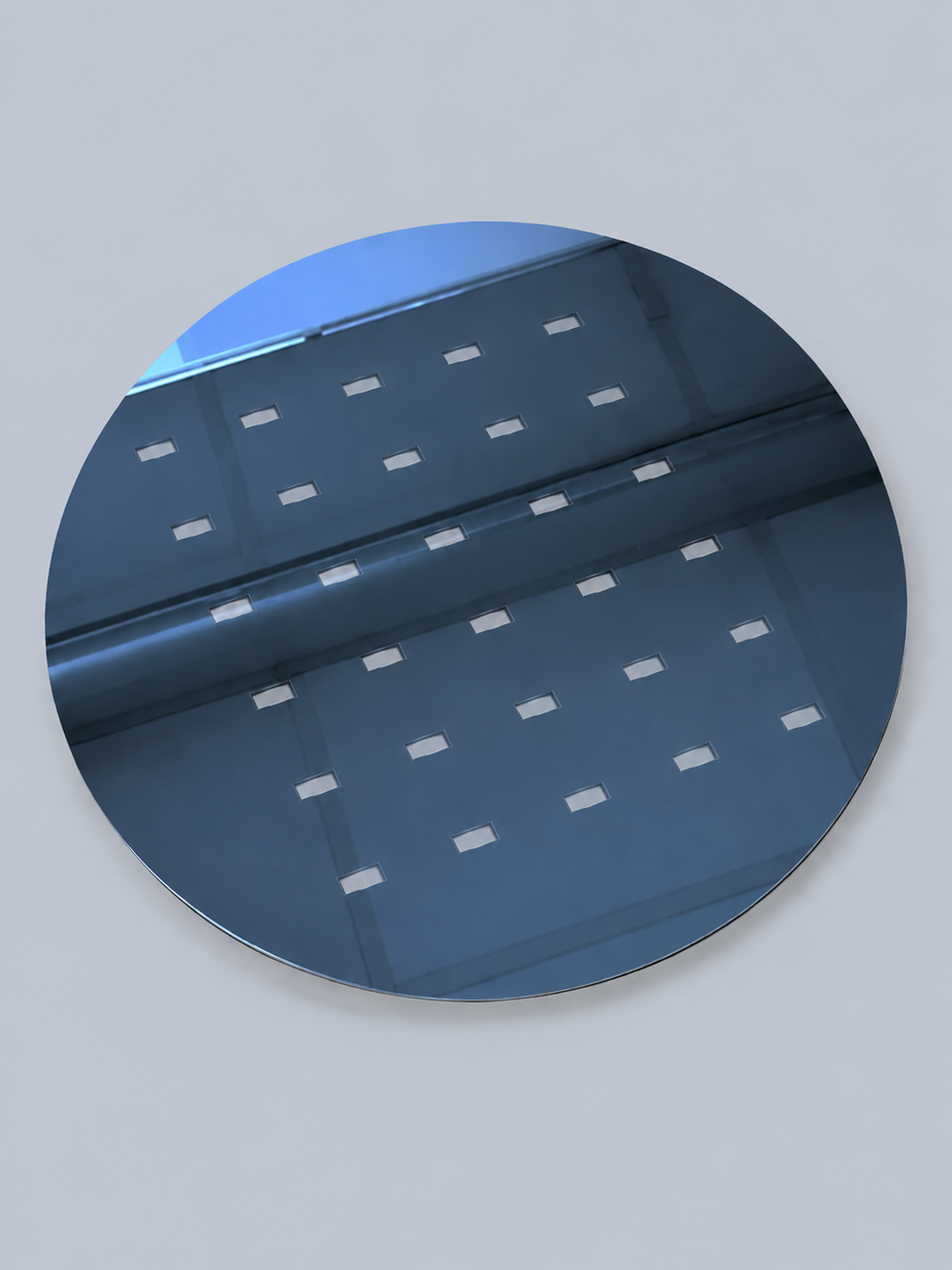
In semiconductor equipment, MEMS devices, sensors, advanced packaging, and specialized photonics applications, silicon wafers with deep cavity or high aspect ratio structures are becoming increasingly common.
These wafers are often referred to as:
- Pocket Wafers
- Cavity Wafers
- Trench Wafers
- Patterned Wafers
- Structured Wafers
After cavity machining, grinding, etching, or trench formation, these wafers often require an additional insulation or oxide layer to support:
- Electrical insulation
- Surface protection
- Plasma resistance
- MEMS structures
- Thin film deposition
- Sensor isolation
- Semiconductor process integration
However, once wafer structures become deeper, thinner, and more complex, insulation layer processing is no longer a simple coating task. Engineers must also consider:
- High aspect ratio coverage
- Sidewall uniformity
- Thermal stress
- Wafer warpage
- Particle contamination
- Film conformality
As a result, semiconductor engineers frequently face an important question:
Which process is more suitable for deep cavity wafers: Thermal Oxide, CVD, or ALD?
This article analyzes the differences, advantages, and limitations of these three common insulation layer processes for deep cavity semiconductor wafers.
Challenges of Deep Cavity Wafers
When a wafer contains:
- Deep cavities
- Fine trenches
- High aspect ratio holes
- MEMS structures
- Deep etched regions
the insulation layer process becomes significantly more difficult compared to standard flat wafers.
One of the biggest challenges is that cavity geometry directly affects gas diffusion, deposition uniformity, and thermal stress control.
High Aspect Ratio Challenges
Aspect ratio is typically defined as:
Aspect Ratio = Depth / Width
As cavity depth increases and opening size decreases, process gases become more difficult to distribute uniformly throughout the structure.
This may result in:
- Insufficient bottom coverage
- Non-uniform sidewall thickness
- Excessive deposition near the opening
- Shadowing effects
- Poor conformal coating performance
These issues become especially important in:
- MEMS wafers
- Deep trench wafers
- Through-silicon vias (TSV)
- Pocket wafers
What is Thermal Oxide?
Thermal Oxide is one of the most traditional and widely used oxide layer processes in semiconductor manufacturing.
The process forms SiO₂ directly on the silicon surface by reacting oxygen or steam with silicon at high temperatures.
Typical process temperatures range from:
900°C to 1100°C
Because the oxide layer grows directly from the silicon substrate itself, Thermal Oxide provides:
- Extremely high film quality
- Excellent electrical properties
- Strong interface quality
- Superior adhesion
As a result, it is widely used in:
- Gate oxide applications
- MEMS insulation layers
- Semiconductor protection layers
- High reliability semiconductor processes
Advantages and Limitations of Thermal Oxide
Advantages
- Excellent Oxide Quality
Thermal Oxide produces highly dense SiO₂ layers with excellent:
- Dielectric performance
- Reliability
- Interface quality
This makes it highly suitable for critical semiconductor applications.
- Strong Adhesion
Because the oxide layer grows directly from the silicon substrate rather than being externally deposited, adhesion is typically superior to many coating processes.
Limitations
- High Temperature Stress
The high process temperature may introduce:
- Wafer warpage
- Thermal stress
- Microcracks
- Bonding layer damage
- Structural deformation
This is especially important for:
- Thin wafers
- Ground wafers
- Bonded wafers
- MEMS wafers
- Limited Uniformity in Deep Cavities
As cavity depth increases:
- Oxygen diffusion becomes less efficient
- Oxide growth rates at the bottom of the cavity may decrease
As a result, thickness uniformity may become more difficult to maintain in high aspect ratio structures.
What is CVD (Chemical Vapor Deposition)?
CVD is one of the most widely used thin film deposition processes in semiconductor manufacturing.
The process uses chemical vapor reactions to deposit thin films onto the wafer surface.
Common types include:
- LPCVD
- PECVD
- APCVD
These processes can deposit materials such as:
- SiO₂
- SiN
- Poly-Si
- Protective coatings
Advantages and Limitations of CVD
Advantages
- Lower Processing Temperature
Especially in PECVD systems, processing temperatures are significantly lower than Thermal Oxide.
This is beneficial for:
- Thin wafers
- Patterned wafers
- Ground wafers
- Faster Deposition Rate
Compared to ALD:
- Higher throughput
- Shorter processing time
- Lower production cost
make CVD more suitable for larger-scale manufacturing.
Limitations
- Reduced Coverage in Deep Cavities
As cavity depth increases, CVD processes may suffer from:
- Shadowing effects
- Reduced bottom coverage
- Sidewall non-uniformity
This is particularly noticeable in PECVD processes.
- Practical Limits for High Aspect Ratio Structures
Theoretical capability does not always translate into stable mass production performance.
Actual process feasibility still depends on:
- Cavity depth
- Opening size
- Aspect ratio
- Film thickness requirements
What is ALD (Atomic Layer Deposition)?
ALD is widely recognized as one of the best thin film processes for high aspect ratio semiconductor structures.
Key characteristics include:
- Atomic-level deposition
- Excellent conformality
- Superior sidewall coverage
- Extremely uniform film thickness
As a result, ALD is increasingly used in:
- MEMS devices
- Deep trench structures
- TSV applications
- Advanced semiconductor manufacturing
Advantages and Limitations of ALD
Advantages
- Best Coverage for High Aspect Ratio Structures
Even in:
- Deep trenches
- Micro holes
- High AR cavities
ALD can still maintain excellent conformal coverage.
This is one of ALD’s biggest advantages.
- Extremely Precise Thickness Control
ALD enables highly precise film thickness control, making it suitable for:
- Advanced MEMS devices
- High-end semiconductor applications
- Precision insulation layers
Limitations
- Longer Processing Time
ALD is a cycle-based process.
As a result:
- Processing speed is slower
- Manufacturing cost is higher
- Thick Films Can Become Expensive
For applications requiring:
- Thick oxide layers
- Large-area coatings
ALD costs may increase significantly.
The Importance of Particle Control and Clean Handling
In semiconductor wafer processing, coating technology alone is not sufficient.
Particle contamination control is equally critical.
When wafers already contain:
- Microstructures
- Deep cavities
- High aspect ratio trenches
- MEMS patterns
even microscopic particles may cause:
- Film defects
- Electrical leakage
- Bonding failures
- Yield reduction
- Downstream process failures
As a result, cleanliness and particle management become especially important during:
- Wafer handling
- Wafer cleaning
- Thin film deposition
- Pocket wafer processing
Which Process is Best for Deep Cavity Wafers?
Each process has different strengths:
| Condition | Recommended Process |
| Highest SiO₂ quality | Thermal Oxide |
| Lower-cost mass production | CVD |
| High aspect ratio structures | ALD |
| Best sidewall conformality | ALD |
| Thin wafers / low-temperature processing | PECVD / ALD |
| Thick oxide layers | Thermal Oxide / CVD |
| Advanced MEMS applications | ALD |
In practice, engineers must evaluate factors such as:
- Cavity depth
- Opening size
- Aspect ratio
- Wafer thickness
- Oxide thickness
- Temperature limitations
- Existing patterns
- Wafer handling methods
- Cleanliness requirements
- Reliability targets
As a result:
Even among Pocket Wafers, different structures may require completely different insulation layer solutions.
Conclusion
For deep cavity wafers and Pocket Wafers, Thermal Oxide, CVD, and ALD each offer unique advantages.
- Thermal Oxide provides extremely high-quality SiO₂ layers but requires careful consideration of high-temperature effects and deep cavity limitations.
- CVD offers better throughput and cost advantages for mass production, but high aspect ratio coverage may become challenging.
- ALD delivers the best conformality for high AR structures, although processing time and cost are typically higher.
In semiconductor manufacturing, there is no single “best” process for every application.
The optimal solution depends on:
- Wafer geometry
- Cavity depth
- Material properties
- Downstream process requirements
- Reliability expectations
Careful engineering evaluation is essential to determine the most suitable insulation layer process for each semiconductor wafer application.
InstaVoxel Semiconductor Wafer Engineering Services
InstaVoxel specializes in precision semiconductor component manufacturing and wafer-related engineering support, including:
- Pocket Wafer Machining
- Wafer Grinding / Back Grinding
- Deep Cavity Wafer Processing
- Advanced Ceramic Machining
- Semiconductor Material CNC Machining
- Wafer Inspection & Metrology
- Semiconductor Process Engineering Support
- DFM Analysis for Semiconductor Components
We also collaborate with semiconductor-related process partners for:
- Thermal Oxide
- CVD / PECVD
- ALD
- Precision Cleaning
- High Cleanliness Handling
to support advanced semiconductor and MEMS applications.
Engineering Note
The images and examples presented in this article are intended to illustrate common engineering concepts and representative industry practices. To protect customer confidentiality, certain dimensions, geometries, specifications, and application details may have been modified while preserving the underlying engineering principles.